
A Few Thoughts on Avoiding DDR4 Layout Problems
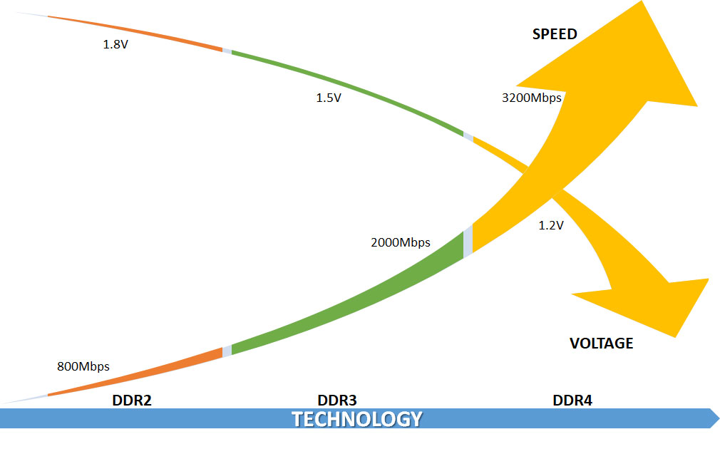
DDR4, the fourth generation of DDR SDRAM technology, is the latest and greatest SDRAM standard and will continue to be until the fifth generation is released. The new standard features a point-to-point architecture that offers superior timing margins. In theory, this should make signal integrity easier to achieve since the designer has more leeway in routing and length matching of the different bit, clock and address lines, assuming operation at the same data rates. But most real-world designs are going to take advantage of DDR4’s ability to double the maximum rate and in this case routability will actually be considerably more challenging than with DDR3.
Overcoming Crosstalk
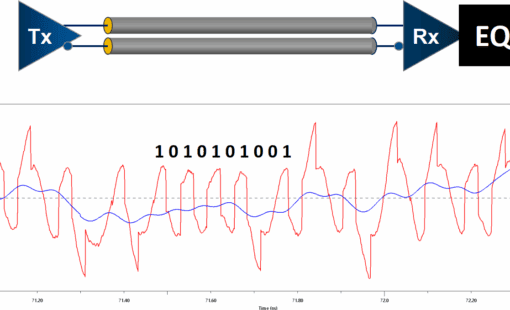
The higher data rates of DDR4 increase the edge rate which in turn increases the propensity for crosstalk. A general rule of thumb is to space out adjacent signal traces at least three times the trace width in order to minimize coupling effects. But it’s often difficult to implement such large trace spacing, especially on smaller PCBs such as those used in smartphones. This conundrum is increased by the fact that SDRAM uses a source synchronous clocking scheme in which all the signals in each signaling group propagate in one direction at the same time. In cases where large trace spacing cannot be achieved, the next best choice is typically to route these traces on stripline – inner PCB layers – instead of microstrip – the outer layer. This is because one side of microstrip does not have a power plane, resulting in greater dispersion of electromagnetic waves which in turn leads to a greater propensity for crosstalk to occur.
Avoiding Vias When Practical
But nothing is simple in PCB design and routing on inner layers can also create complications when DDR4 signals travel through vias from one layer of a PCB to another. Capacitance and losses in the vias can produce signal integrity problems, especially in the short stubs formed by the extension of the vias plating through to the other side of the PCB. One approach to address this problem is to minimize layer changes by routing mainly in the outer layers to avoid layer changes. But since, as mentioned earlier, routing on the outer layer increases the tendency towards crosstalk, other measures may be necessary. For example, backdrilling with numerically controlled drills to reduce the via stub length can significantly lower the bit error rate of the interconnect.
Tune the Silicon to the Board
Cases where designers have control over the silicon provide an additional avenue to address potential DDR4 problems. Devices such as field programmable gate arrays (FPGAs) enable engineers to move pins around to reduce trace lengths. While ICs, packages and PCBs are typically designed with point tools whose interface requires time-consuming manual processes, a new integrated 3D chip/package board co-design environment enables engineers to see the IC, package and PCB simultaneously in one view to optimize tradeoffs between the pin placement and PCB routing, among other things. This new approach makes it much easier to, for example, swap pins between banks, to achieve better length control.

-
Solution architect


- Blog
Modern electronic products are no longer built around a single PCB. As systems become faster, denser, and more interconnected, engineering teams are being forced to rethink how they design, verify, and manage complex multi-board products.
- Blog
Explore how CR-8000 enhances PCB design with integrated control of impedance and resistance—enabling precise analysis for both high-speed and high-power applications, from signal integrity to power distribution optimization.

- Blog
High-Speed-Serial-Links wirken oft wie schwarze Magie – steigende Datenraten verstärken dieses Gefühl. Donald Telian (SI Guys) und Ralf Brüning holen die Diskussion zurück zu den Grundlagen.
- Blog
Lerne die beiden wichtigsten Grundlagen für den zuverlässigen Entwurf von High Speed Serial Links und erfahre, wie du Herausforderungen bei der Signalintegrität bei Geschwindigkeiten von mehreren Gbit/s meistern kannst.