Double Data Rate 5 (DDR5) is the next-generation standard for random-access memory (RAM). The new specification promises to bring chips that have much higher performance than the existing DDR4 modules, as well as lower power consumption. Let us show you how you can be first to market with DDR5 design!
DDR5 performance
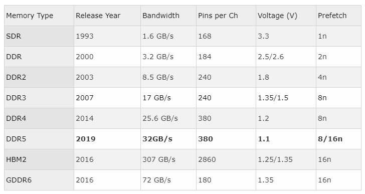
DDR5 designs promise to arrive on the market with double the density as well as double the performance of the first-generation DDR4 modules.

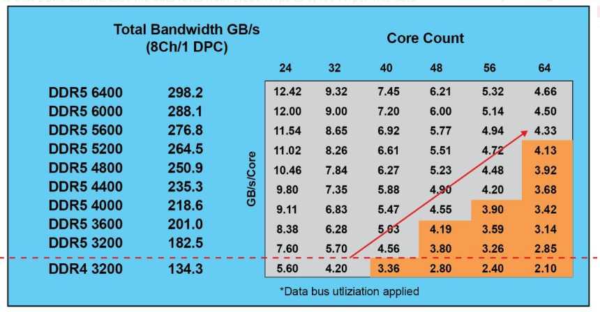
DDR5-3200 RAM will see an increase of 1.36x in bandwidth compared to DDR4-3200. However, DRAM chips are expected to ship with a bandwidth of 4800MT/s, or 1.87x that of DDR4-3200 RAM. The official upper limit for the DDR5 RAM standard is 6400MT/s, but some designs may be able to push that further through overclocking.
SK Hynix has been working on DDR5 modules that can deliver 16Gb (2GB) capacity per chip. The company lowered voltage from 1.2V to 1.1V, which combined with the usage of its 1Ynm process, reduced power consumption compared to the company’s DDR4 modules. The module offers up to 6.4Gb/s of throughput for each pin.
Other benefits of DDR5 RAM include two independent 40-bit channels per module, improved command bus efficiency, improved refresh schemes, and an increased bank group for additional performance.
Features enabling high-bandwidth DDR5 RAM
According to Micron, DDR5 designs will use a completely overhauled architecture compared to DDR4, with a focus on increasing bandwidth. A number of key features enable this increase in bandwidth. The most important is that DDR5 can increase the data rates from 3,200 MTps to 6,400 MTps. This data rate increase alone should more than keep up with potential future processors with even more cores.

With great technical ambitions come much tighter specifications for system PCB designers; especially when faced with channel loss, skew, reflections and crosstalk, all of which become much more significant at higher frequencies. In fact, PCB design margins are so minimal that DDR5 introduces equalization on the commodity DRAM chips, for the first time.
Are you ready for DDR5?
Zuken and Keysight join together in this on-demand webinar. Our subject matter experts will help you navigate key technical concerns as you embark on your first DDR5 design. In this webinar, we will explore a predictive, productive, and insightful workflow to get to an optimal design that performs to the target speed grade reliably. We’ll begin with pre-layout simulation to explore design choices, then transition to constraint-based high-speed routing. Finally, we will verify the design by electromagnetic (EM) simulation and system simulations to build confidence in the final DDR5 design.
What you will learn:
- The main differences between DDR5 to previous generations
- Why pre-layout simulation is necessary to arrive at an optimal design (using Keysight’s PathWave ADS)
- How to use constraints in Zuken’s CR-8000 to setup routing quickly
- How to estimate crosstalk in Zuken’s CR-8000
- What is important to know about accurate electromagnetic model extraction of the PCB (using Keysight’s SIPro in PathWave ADS)
- How to perform system-level simulations to determine signal integrity and reliability of a design
Who should attend:
Technical and electrical design engineers, engineering managers, PCB designers, academic researchers, and students.


