PCB Design
Menu

- Blog
März 29, 2018
Controlling the Release Points for Your PLM/PDM System
There is one thing that all design engineers will agree on: creating and gathering all the required data for PLM is error-prone and can be a royal pain. We all understand the value of releasing our design data to the corporate PLM system but our design process dictates multiple release points, and each one has a different purpose and data requirements.
Read now
There is one thing that all design engineers will agree on: creating and gathering all the required data for PLM is error-prone and can be a royal...

- Blog
März 22, 2018
Mastering Power Integrity: First Get Your Power Distribution System Right
I don’t think I’m generalizing when I say that designers working on complex high speed designs really don’t want to expend a lot of time and effort dealing with power integrity problems. And they especially don’t want to do it using tools that are detached from their design flow. In today’s complex PCBs, we’re talking advanced processors, complex FPGAs and superfast memories, which all share various voltage ranges.
Read now
I don’t think I’m generalizing when I say that designers working on complex high speed designs really don’t want to expend a lot of time and...

- Blog
März 01, 2018
Lower Manufacturing Costs with XJTAG’s New Design Gateway Plugin
PCB Design, Boundary Scan, CR-8000 Design Gateway, Manufacturing Design Technology, Partners and Integrations, Blog
XJTAG has partnered with Zuken create a new plugin for Design Gateway and is offering it free of charge. The plugin, called XJTAG DFT Assistant, h...

- Blog
Februar 08, 2018
EMC = DRC²: The Importance of EMC Rule Checking
When it comes design rule checks for PCB designs, there are checks that should be performed that are just as important as spacing rules. Strict adherence to basic PCB design rule checks, such as track to track, track to via, via to via, pad to track etc. – though necessary to avoid short circuits – only scratch the surface when trying to identify potential design flaws.
Read now
When it comes design rule checks for PCB designs, there are checks that should be performed that are just as important as spacing rules. Strict ad...
- Blog
Januar 25, 2018
Advanced Packaging with Zuken’s CR-8000 Design Force
Advanced packaging techniques such as system-in-package (SiP), fan-out wafer-level packaging (FOWLP), 3D die stacks, etc. have been around for over a decade, yet with any other EDA design tool, it is still a tedious, time consuming, and error-prone process to implement these designs.
Read now
Advanced packaging techniques such as system-in-package (SiP), fan-out wafer-level packaging (FOWLP), 3D die stacks, etc. have been around for ove...

- Blog
Januar 18, 2018
Four Steps for Avoiding Surprise In-Use Product Failures
As we witness the birth of an era of connected devices with smart homes, connected cars and smart networked supply chains and factories, we might imagine that unexpected failures of electronic products would be a rarity.
Read now
As we witness the birth of an era of connected devices with smart homes, connected cars and smart networked supply chains and factories, we might ...

- Blog
Dezember 07, 2017
How Virtual Prototyping Tools Can Help Decide if Fan-out Wafer-level Packaging is Right For Your Product
Since it contributed to making the iPhone 7 even thinner than its predecessors, fan-out wafer-level packaging (FO-WLP) technology has risen in the collective consciousness. By adopting FO-WLP on this scale, Apple sent out a signal that though highly novel, the technology had matured.
Read now
Since it contributed to making the iPhone7 even thinner than its predecessors, fan-out wafer-level packaging (FO-WLP) technology has risen in the ...

- Blog
November 16, 2017
What High Tech Industries Can Learn about Managing Data from the Early Days of CAD
Because I’ve been in the electrical/electronics (E/E) engineering industry for such a long time, I can still remember drawing PCB layouts manually. We would then work out the connection lengths of wire harnesses by laying out waxed cord lacing on a physical prototype.
Read now
Because I’ve been in the electrical/electronics (E/E) engineering industry for such a long time, I can still remember drawing PCB layouts manual...
- Blog
November 13, 2017
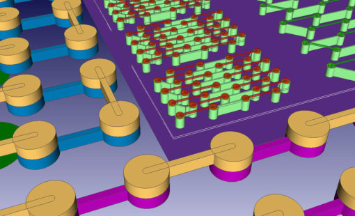
Toshiba – RF Module Shrink (TransferJet™)
Toshiba faced a difficult design problem: their TransferJet™ technology was embedded in a customer cell phone, and when the next rev of the phone came around, they learned that they needed to shrink the board from 8mm x 8mm to 4.5mm x 6mm, and they had to shrink the module thickness from 1.7mm to 1.0mm...
Read now
Toshiba faced a difficult design problem: their TransferJet™ technology was embedded in a customer cell phone, and when the next rev of the phon...
- Blog
Oktober 11, 2017
The Challenges of 3D PCB Designing (PCB West Interview)
During PCB West Exhibition Day, Sierra Circuits met Humair Mandavia, Chief Strategy Officer at Zuken. After his joint interview with Simon Fried, CBO of Nano Dimension, we discussed 3D PCB designing, and Zuken’s product, CR-8000 with him.
Read now
During PCB West Exhibition Day, Sierra met Humair Mandavia, Chief Strategy Officer at Zuken. After his joint interview with Simon Fried, CBO of Na...

- Blog
Oktober 09, 2017
How to Improve Flexible Printed Circuit Manufacturing (PCB West Interview)
Sierra met Steve Watt, Manager of PCB Engineering at Zuken, during PCB West 2017 at the Santa Clara Convention Center. After his presentation on how to improve flexible printed circuit manufacturing, he shared a few tips in front of our camera. Listen to him discuss CR-8000, DfM checks, and flexible PCB designing.
Read now
Sierra Circuits met Steve Watt, Manager of PCB Engineering at Zuken, during PCB West 2017 at the Santa Clara Convention Center. After his presenta...

- Blog
September 26, 2017
Improve Design Data Security Across Your Enterprise
This is one pretty scary world we live in. Every day there are stories about data breaches, network hacks and even possible spying by foreign software and hardware suppliers. Every individual has become hyper-aware of the security issues revolving around their personal data. A company’s need to protect its design IP is actually more critical than an individual’s need to protect their personal data.
Read now
It is essential to insure that you are taking the necessary steps to maximize your product revenue while protecting your company’s intellectual ...
- Blog
September 19, 2017
25 Years of High Speed Design – Looking Back to the Future
It’s 25 years since the first FED Conference took place in Berlin back in 1993, as a gathering for the German-speaking electronic and PCB-related industry. This also happened to be the year we consider as the birth of high-speed design.
Read now
It’s 25 years since the first FED Conference took place in Berlin back in 1993, as a gathering for the German-speaking electronic and PCB-relate...

- Blog
September 15, 2017
Does the Release Process to Manufacturing Keep You Up at Night?
Have you ever finished generating the manufacturing release package for the latest product design and then it occurred to you that something may be wrong? Imagine, it’s Thursday night and you just finished a nice dinner with the family. Your daughter’s soccer team won and the Broncos are playing the Chiefs tonight. It will be great to relax and enjoy the game.
Read now
Have you ever finished generating the manufacturing release package for the latest product design and then it occurred to you that something may b...

- Blog
August 29, 2017
A Few Thoughts on Avoiding DDR4 Layout Problems
DDR4, the fourth generation of DDR SDRAM technology, is the latest and greatest SDRAM standard and will continue to be until the fifth generation is released. The new standard features a point-to-point architecture that offers superior timing margins.
Read now
This new approach makes it much easier to, for example, swap pins between banks, to achieve better length control.

- Blog
August 22, 2017
Translating New Product Requirements into Hardware Architecture
Defining initial hardware architecture requires many decisions, most of which impact a variety of different stakeholders and requirements – including multiple design tools – circuit design, PCB layout, mechanical design, spreadsheets, etc. that are used to track different elements of the design.
Read now
Defining initial hardware architecture requires many decisions, most of which impact a variety of different stakeholders and requirements – incl...