PCB Design
Menu

- Blog
August 02, 2017
Hardware Architecture Design Becomes the Next Competitive Requirement
After a lengthy quiet period, the hardware design process is suddenly experiencing numerous changes in the form of design discipline convergence and process extension. The widely used 2D single board PCB detailed design process is being replaced by a 3D multi-board and multi-discipline one.
Read now
Hardware architecture design is becoming a competitive requirement as product complexity is on the rise and the room for error is shrinking.

- Blog
Juli 14, 2017
Renishaw Designs Flex PCBs in True 3D with MCAD Integration using Zuken's CR-8000
The PCB design team at Renishaw work with flex PCBs and flexi-rigid boards that require detailed signal integrity analysis. To achieve the most accurate results they are working with Zuken’s electronic PCB design software to visualize boards in 3D using imported MCAD data. This also ensures that sure high-speed digital signals can be transmitted with minimal distortion.
Read now
When Renishaw decided to migrate to Zuken’s latest PCB design suite in 2016, a main driver was the suite’s capabilities for designing and anal...

- Blog
Juni 21, 2017
Predictive Failure Analysis Can Improve Product Quality: The Reality - Part 2 of 2
I recently talked on predictive failure analysis at the PTC LiveWorx 2017 conference. There was a lot of audience interest, so I thought I’d share some of the things I discussed. This is the second of two posts on this subject.
Read now
We all know that manufacturing yields and costs are the driving force behind product development, rather than product quality.

- Blog
Juni 15, 2017
Predictive Failure Analysis Can Improve Product Quality - Part 1 of 2
I recently talked on predictive failure analysis at the PTC LiveWorx 2017 conference. There was a lot of audience interest, so I thought I’d share some of the things I discussed.
Read now
The good news is that more and more devices are becoming part of the Internet of Things (IoT), which extends the design team’s visibility beyond...

- Blog
Juni 06, 2017
Design Time vs. Admin Overheads: How to Win the Battle by Closing the Gaps
No more distractions, please! 45% of our time is already spent on admin. If you’re the average engineer, that is.
Read now
Techconsult, a German-based analyst firm has just found that almost half of the engineering time of any manufacturing company is spent feeding sys...

- Blog
März 03, 2017
Growing Pains in the Wearables Market
With key functionality in many cases commoditized, the success or failure of wearables is increasingly determined in the early stages of the PCB and mechanical integration process where requirements are translated into practical design decisions such as how functions are mapped to PCBs and PCBs are integrated into the enclosure.
Read now
With key functionality in many cases commoditized, the success or failure of wearables is increasingly determined in the early stages of the PCB a...
- Blog
Januar 27, 2017
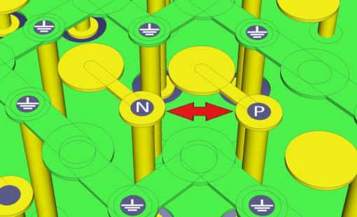
Return Vias, Build-Up Layers and the Latest FPGAs to Battle Latest Signal Integrity Challenges
In the final installment of this blog series, you can learn how to use build-up layers and premium FPGAs to deal with the signal integrity challenges arising from high-speed signals in a 3D design capture world.
Read now
Luckily, where signals need return vias, component vendors often do most of the work for you. Let’s look at a PCI Express differential pair. Fi...
- Blog
Januar 19, 2017
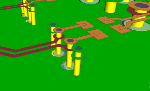
Using Vias to Maintain PCB Signal Integrity Featuring High-Speeds in a 3D Environment
This is the second in my series of blog posts looking at the challenge of maintaining PCB signal integrity with now-common ultra-high speeds and growing adoption of PCB design environments to design in true 3-D. Today I focus on vias and the use of return vias to overcome the issues highlighted in Part 1.
Read now
This is the second in my series of blog posts looking at the challenge of maintaining PCB signal integrity with now-common ultra-high speeds and g...
- Blog
Januar 12, 2017
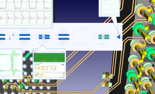
The High-Speed Design Challenge of Maintaining PCB Signal Integrity in a 3D Design Environment
Ultra-high signal speeds demand detailed consideration of the third dimension in PCB design, including via structures and layer stacks. Today I’m going to focus on the challenge. In my two subsequent posts I’ll be reviewing what PCB designers can do to meet that challenge.
Read now
Ultra-high signal speeds demand detailed consideration of the third dimension in PCB design, including via structures and layer stacks. Today I’...

- Blog
März 17, 2016
Circuit Modular Reuse Best Practices
In my previous post in this series about effectively reusing design modules to increase product quality and decease development time, I challenged you to think about how well you’re making use of existing design modules and why getting better at this could be a competitive differentiator.
Read now
In my previous post in this series about effectively reusing design modules to increase product quality and decease development time, I challenged...

- Blog
März 11, 2016
Are you Making the Most of Modular Design With Design Reuse? Part 1
In this two part series of blog posts, I’m going to be looking at reuse with modular design in PCB development, and how you can streamline your methodology to reduce design time, reduce design errors and increase product quality.
Read now
Although we’ve been talking about it for years, in PCB design it has yet to catch on in quite the same way despite there being a host of benefit...

- Blog
September 11, 2013
How to Protect PCB Design Intellectual Property
As companies benefit from the global supply chain in terms of lower production costs and faster turnaround times, they are also exposing their intellectual property to third parties, including PCB design data.
Read now
It’s easy to get complacent about this topic, but it’s important to remember that a company’s IP is often the basis for its competitive adva...
- Blog
August 20, 2013
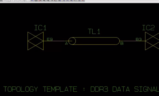
Defining and Routing PCB Constraints for DDR3 Memory Circuits: How-to Movies
As Zuken technology partners, we are often asked about how best to set PCB constraints for double-data-rate (DDR) memory, and how to route to those constraints. This question arose recently when we were asked to create a common style of DDR3 design for training, and we tried mining the web for detailed information on PCB constraints. There had to be something out there, we thought.
Read now
As Zuken technology partners, we are often asked about how best to set PCB constraints for double-data-rate (DDR) memory, and how to route to thos...

- Blog
November 09, 2010
S-Parameters: Microwave goes Mainstream for High-Speed PCB Design Part 2
Previously I introduced you to the concept of S-Parameters, and now I’m going to explain a bit more about measuring them and simulating with S-Parameter models.
Read now
Last week I introduced you to the concept of S-Parameters, and now I’m going to explain a bit more about measuring them and simulating with S-Pa...

- Blog
November 01, 2010
S-Parameters: Microwave goes Mainstream for High-Speed PCB Design Part 1
I’d like to explain to you in straightforward terms what S-Parameters are and why they’re so useful. When I say “straightforward”, I mean that in a technical sense, but this is a specialised area. If you’re not designing high-speed PCBs, or you don’t know much about signal integrity, you might want to tune out now.
Read now
So here goes. Mainstream high-speed PCB design has generally followed in the slipstream of RF and microwave engineering. This is often out of nece...