Defining and Routing PCB Constraints for DDR3 Memory Circuits: How-to Movies
As Zuken technology partners, we are often asked about how best to set PCB constraints for double-data-rate (DDR) memory, and how to route to those constraints. This question arose recently when we were asked to create a common style of DDR3 design for training, and we tried mining the web for detailed information on PCB constraints. There had to be something out there, we thought.
We were right; but unfortunately the detail had to be excavated from a vast and comprehensive pile of information about devices and controllers. It was hard to find a brief but clear description of what a PCB designer needs, and why, for a basic DDR3 circuit.
PCB Design of a DDR3 Memory Circuit
Necessity being the mother of invention I worked with Kevan Keech, an expert PCB designer, to create the most straightforward, realistic example we could think of – captured in three short movies.
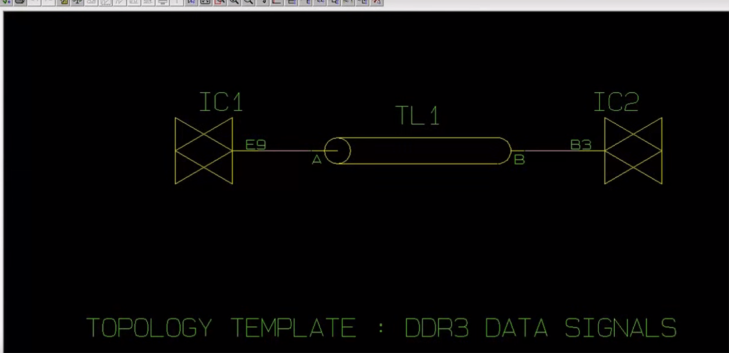
In the first movie I explain the circuit, routing topology and constraints.
In the second movie, Kevan constrains the PCB design.
In the final movie, Kevan routes the PCB design step-by-step and at the end we summarize the results.
We use a single design example from start to finish – a controller connected to five 1-Gbitx8 SDRAM devices. Levelling is enabled so that the SDRAMs can be routed using fly-by topology, as defined in JEDEC standards and elsewhere.
After watching these movies, you will understand:
- What key routing constraints you need for a memory circuit, such as that outlined in the movies
- How to adjust routing to balance impedance of lead-in and loaded sections as specified in JEDEC standards and why you might need to do so
- How to place SDRAM components for optimum performance
- How to constrain the PCB design
- How to route accurately to DDR3 constraints
- How to ensure constraints have been met.
We hope you enjoy the movies and find them useful.
If you’ve taken a look, why not leave a comment below!

-
Electronic Design Technology Partner


- Blog
Explore how CR-8000 enhances PCB design with integrated control of impedance and resistance—enabling precise analysis for both high-speed and high-power applications, from signal integrity to power distribution optimization.

- Blog
High-Speed-Serial-Links wirken oft wie schwarze Magie – steigende Datenraten verstärken dieses Gefühl. Donald Telian (SI Guys) und Ralf Brüning holen die Diskussion zurück zu den Grundlagen.
- Blog
Lerne die beiden wichtigsten Grundlagen für den zuverlässigen Entwurf von High Speed Serial Links und erfahre, wie du Herausforderungen bei der Signalintegrität bei Geschwindigkeiten von mehreren Gbit/s meistern kannst.

- Blog
CR-8000 2025 integrates AI to support constraint-driven PCB design - offering layout guidance, reusable knowledge, and schematic consistency without removing the engineer from the loop.