Advanced packaging techniques such as system-in-package (SiP), fan-out wafer-level packaging (FOWLP), 3D die stacks, etc. have been around for over a decade. Yet with any other EDA design tool, it is still a tedious, time-consuming, and error-prone process to implement these designs.
It seems surprising that there are so few reliable EDA solutions out there. But CR-8000 Design Force is definitely the tool to look to when tackling advanced package design! Take a look below and see why.
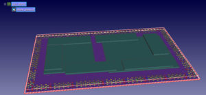
CR-8000 Design Force was architected as a hierarchical printed circuit board and integrated circuit package design database. The image below shows an example of a package-on-package (PoP) design. The lower package contains two ASICs, while the upper package has six memories. You can easily switch from substrate to substrate and make design changes. Pin swaps at the shared pins are passed seamlessly between the designs.
The natural hierarchical and 3D architecture of this tool makes it simple to create any type of advanced package design you can imagine. At the recent IWLPC conference in San Jose, Samsung presented on Fan-out Panel Level Packaging. CR-8000 Design Force is the natural choice for this type of design as it doesn’t require re-tooling (or re-coding) to make it work!
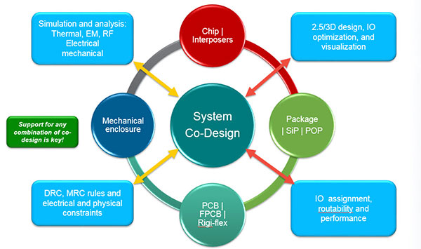
CR-8000 Design Force enables co-design between all parts of the design in an intuitive flow. Not just IC package co-design functionality in a separate design environment, but co-design natively built into the software’s DNA. With CR-8000 Design Force, you don’t need a separate co-design tool. It provides package-to-package co-design; IC-package; package-to-board; board-to-board; board-on-board; board-to-assembly panel; co-analysis between layout and analysis tools, and data exchange with 3rd-party EDA vendors. The image below illustrates the “co-design is everywhere” concept.
Advanced Packaging Examples
Let’s take a look at some specific examples of design capabilities in CR-8000 Design Force.
IC-Package Co-design
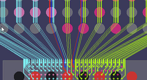
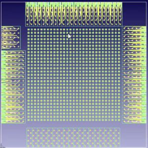 The first example is an IC-driven co-design scenario. The package design team imports the I/O driver placement through LEF/DEF import, creates a bump pattern for the IC, and optimizes the bump pattern and the package connectivity in Design Force. The IC design is all done in a native OpenAccess environment (inside Design Force, no less!).
Pin assignments are made to the package, and optimization of pin assignments operates in a bidirectional manner between the IC and the package.
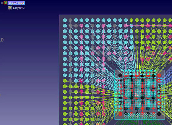
The final result is a clean pathway from I/Os to package balls. Any changes to the die are exported to a DEF file.
Package-on-Package Clearance and Collision Checks
The second example is a Package-on-Package (PoP) design flow. It demonstrates collision and clearance checks between devices on the top and bottom packages of a PoP design. These components are imported either from LEF/DEF, or are fixed components in a library. In the video, the top package has a memory device on its underside, and the bottom package has an ASIC on the top layer. The movie shows collision and clearance checks between the devices. This functionality is especially useful in designs with many passive components on the facing boards to ensure collisions do not occur when the part is assembled.
Daisy Chain Test Chip
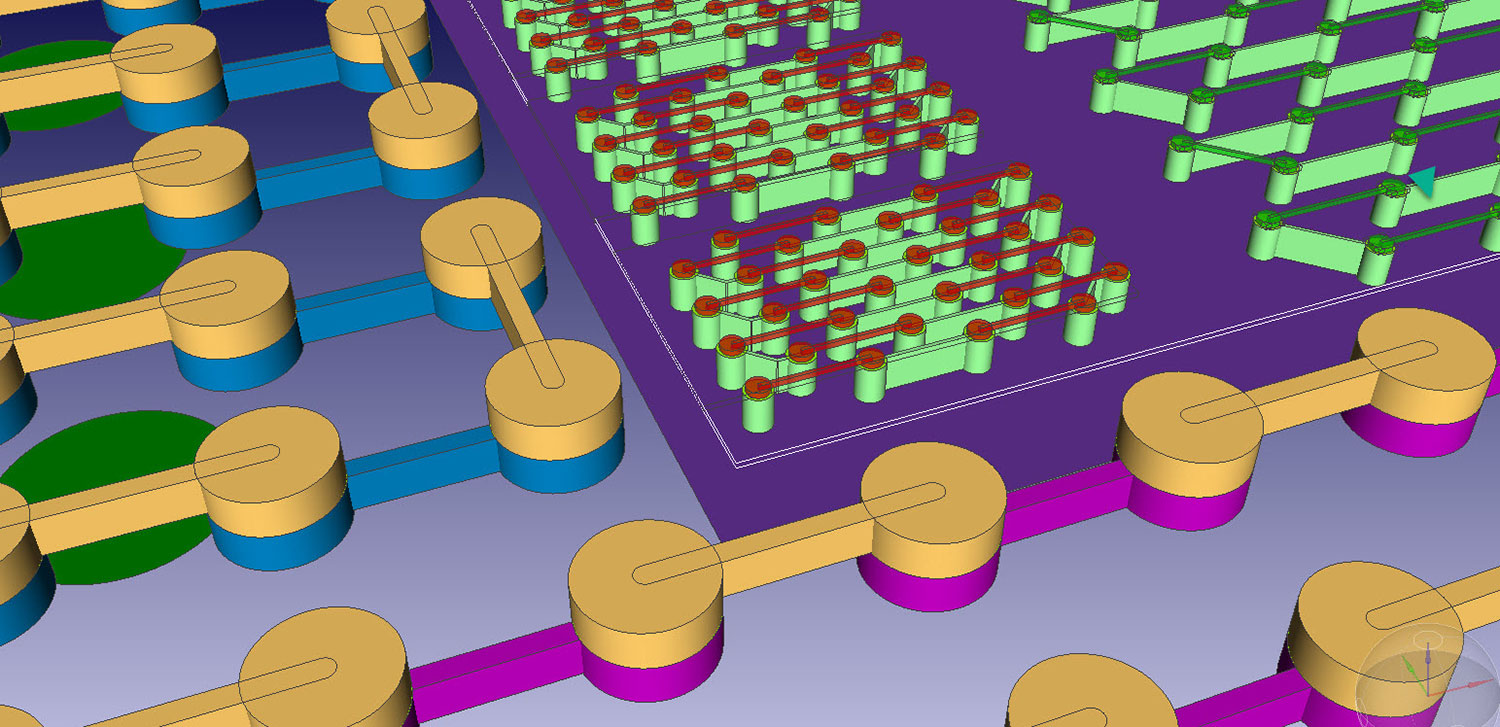
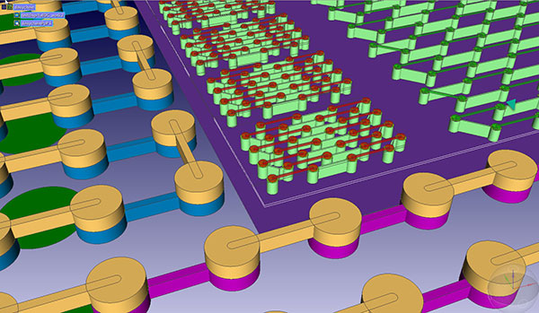
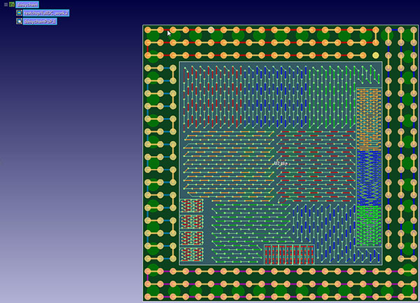
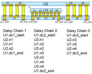 The final example illustrates the creation of a daisy chain test configuration between two packages and between a package and a die in a PoP design. A daisy chain test configuration is a stitching of pins between two (or more) different components. It provides a nearly zero-Ohm path between a set of pins and is used for a variety of tests to validate and improve the assembly process. The image below shows a simple example of two daisy chains (daisy chains 1 and 3) between two packages in a package-on-package configuration. It also shows a single daisy chain (daisy chain 2) between a flip-chip die and the bottom package.
Creating this type of netlist is a tedious and error-prone process with most tools. However, because CR-8000 Design Force is naturally a 3D, hierarchical design system, it provides an easy-to-use utility to create and visualize complex daisy chain configurations. The chain is created or modified by selecting a set of pins and running the command. The netlist for both sets of pins is created (or updated) and the routing for both substrates is created.
A Matter of Minutes
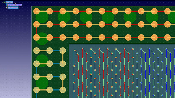
The first example below shows a 2D view of a PoP design with a single flip-chip. There are four daisy chains between the two packages around the perimeter, and there are 15 daisy chains between the die and the bottom package. This design could take days or weeks to complete, but CR-8000 Design Force only takes minutes to complete all chains and routing!
Summary
CR-8000 Design Force is a powerful environment that provides hierarchical design layout and assembly, 3D and 2D design views that enable the assembly of complex packages and PCB configurations in one database, and in one design canvas. Because of this, creating a package-on-package fan-out wafer level design, or a complex PCB, package, and die stack up is rather simple to do. Complex daisy chain designs are quickly completed.
Memories in a top package can easily drive the pinout of ASICs in a bottom package. Connectors on a PCB can drive net assignment to die pins in a die stack. 2D and 3D modes provide an intuitive, dynamic window into the layout of the design. Collision checks and clearance checks provide a view into the 3D space of your design. Design Force is the tool of choice for anyone designing advanced packages of all types.
