Getting IoT Device Design Right for EMC and the ‘Interference of Things’
As we welcome increasing numbers of IoT devices into our industries, offices and home lives, we shouldn’t be surprised to see increasing electromagnetic (EM) congestion. Or, as it’s now dubbed, the ‘Interference of Things’.
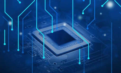
This is because the majority of IoT devices are wireless, and many use multiple communications protocols – WiFi, Bluetooth and Zigbee – to interface with other devices, routers and the Cloud. Creating an IoT device requires a rich mix of design elements and disciplines, including digital and analogue, electromechanical (e.g. actuation), mixed-signal transducers (sensors) and RF.
Consider the whole device
From an EMC perspective, the entire IoT device needs to be considered – rather than a single PCB in isolation. Indeed, a typical IoT device is a 3D multi-board design challenge, where some of the boards might be flexible. The flexi materials and the shapes they form when flexed will all contribute to the device’s EM profile in terms radiation and susceptibility.
However, many of the common-sense PCB design rules that serve us so well in other industry sectors don’t necessarily apply to IoT. For instance, you’re not going to find a large loop antenna on a PCB that’s (say) no larger than a postage stamp. Similarly, the small form-factors will give you little freedom when it comes to the placement and separation of components, or the luxury of shielded tracks, to reduce cross-talk.
Instead, greater emphasis must be placed on grounding practices and, if possible, the isolation of inputs – particularly those from sensors.
If space and budget permit, filtering is beneficial for ensuring a proper and stable power supply and for preventing DC noise. Efficient bypassing and power distribution system optimization are important too.
Get rid of ‘sticking plaster’ components
Adherence to these EMC rules for IoT should mean additional components aren’t needed – those we use for fixing EMI issues which don’t contribute to the circuit’s ideal behavior. Indeed, with smaller form-factors being the norm, you’ll be fighting for every square millimeter of board real estate.
Increasing the number of components or board layers to combat EMI can easily tip a project from high to low profitability because of the additional material costs and delayed product launch dates.
Also, the additional components will almost certainly impact the overall power consumption and could result in thermal issues. That said, you’re probably designing with low power in mind anyway as most IoT devices are battery-powered or have a battery for back-up purposes.
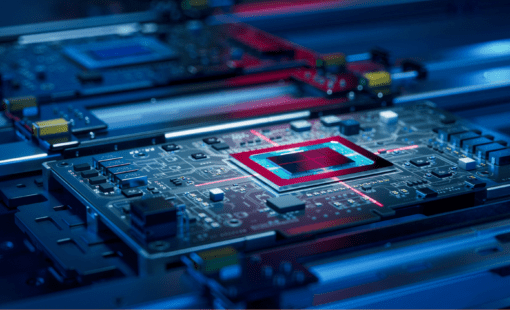
In this respect, most device manufactures provide recommendations for track impedances, and tools like CADSTAR and CR-8000 can show predicted impedances.
Prevention is better than cure
Granted, we’re in the relatively early stages of the IoT boom, but devices are already having to operate in an EM noisy world – one that’s only going to get noisier – and EMC design rules have already changed. For IoT, the strategy is one of prevention not cure. Except for components required to filter inputs and stabilize power, all other components should be there for the core functionality of the device, and not to fix issues that should have been designed out.
So, to sum up. From an EMC perspective, you should design IoT devices with the following in mind:
- The entire device (not just a board or module)
- Low power consumption
- Good signal and power integrity
- Crosstalk control
- Compliance.

-
Product Manager/Senior Consultant


- Blog

- Blog
Executives’ Perspectives on Digital Transformation #5
- Blog
Explore how CR-8000 enhances PCB design with integrated control of impedance and resistance—enabling precise analysis for both high-speed and high-power applications, from signal integrity to power distribution optimization.

- Blog
Build accurate dynamic cables in E3.series by defining cores, shields, and twisted pairs so schematics, reports, and formboard outputs stay consistent.