
How to Calculate Trace Length from Time Delay Value for High-speed Signals
Calculating signal speed on a PCB
According to physics, electromagnetic signals travel in a vacuum or through the air at the same speed as light, which is:
Vc = 3 x 10⁸M/sec = 186,000 miles/second = 11.8 inch/nanosecond
A signal travels on a PCB transmission line at a slower speed, affected by the dielectric constant (Er) of the PCB material. The transmission line structure also affects the signal speed.
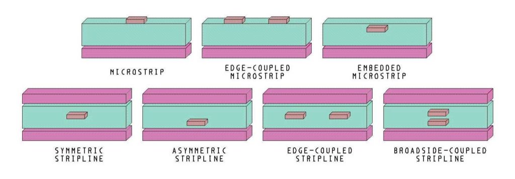
There are two general PCB trace structures [note*]: stripline and microstrip.
The formulas for calculating the signal speed on a PCB are given below:
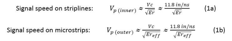
Where:
- Vcis the velocity of light in a vacuum or through the air
- Er is the dielectric constant of the PCB material
- Ereffis the effective dielectric constant for microstrips; its value lies between 1 and Er, and is approximately given by:
Ereff≈(0.64 Er+ 0.36) (1c)
With those formulas, we know that the speed of signals on a PCB is less than the signal speed through the air. If Er≈4 (like for FR4 material types), then the speed of signals on a stripline is half that of the speed through the air, i.e., it is about 6 in/ns.
How to calculate propagation delay (tpd)
The propagation delay is the time a signal takes to propagate over a unit length of the transmission line.
Here is how we can calculate the propagation delay from the trace length and vice versa:
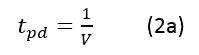 Where:
- Vis the signal speed in the transmission line
In a vacuum or through the air, it equals 85 picoseconds/inch (ps/in).
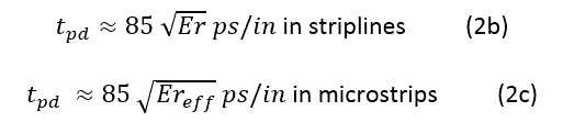
On PCB transmission lines, the propagation delay is given by:
Case study: Calculating trace length on a PCB
In order to be compliant with the specification of JEDEC, the maximum skew among all the signals shall be less than +/-2.5% of the clock period driven by the memory controller. All the signals of SDRAM are directly or indirectly referenced to the clock.
In this example, the normal FR4 material with a dielectric constant of 4 is used on the PCB with a differential clock rate of 1.2GHz (i.e., 833ps clock period):
Question: What is the maximum skew of the trace length for all the signals?
Answer: Max skew in time delay = +/-2.5% of the 833ps clock period = 20.825ps FR4 Er≈4, Ereff≈2.92
So, for strip lines, the maximum skew should be less than +/- (20.825/(85*SQT(4))=+/-0.1225 in = +/- 122.5 mil.
For microstrips, the maximum skew should be less than +/- (20.825/(85*SQT(2.92)) = +/-0.1433 in = +/- 143.3 mil.
Note*: Different microstrip and stripline structures will affect the signal speed, but only slightly.
Keep this information in mind the next time you’re calculating trace lengths; it should make the job a little easier for you.
References:
– Signal Speed and Propagation Delay in a PCB Transmission Line, Atar Mittal
– JEDEC
Also see:
CR-8000 – PCB Design Software Overview

-
Solutions Architect


- Blog
Modern electronic products are no longer built around a single PCB. As systems become faster, denser, and more interconnected, engineering teams are being forced to rethink how they design, verify, and manage complex multi-board products.
- Blog
Explore how CR-8000 enhances PCB design with integrated control of impedance and resistance—enabling precise analysis for both high-speed and high-power applications, from signal integrity to power distribution optimization.

- Blog
High-Speed-Serial-Links wirken oft wie schwarze Magie – steigende Datenraten verstärken dieses Gefühl. Donald Telian (SI Guys) und Ralf Brüning holen die Diskussion zurück zu den Grundlagen.
- Blog
Lerne die beiden wichtigsten Grundlagen für den zuverlässigen Entwurf von High Speed Serial Links und erfahre, wie du Herausforderungen bei der Signalintegrität bei Geschwindigkeiten von mehreren Gbit/s meistern kannst.
Related Content

- Blog
Double Data Rate 5 (DDR5) is the next-generation standard for random-access memory (RAM). The new specification promises to bring chips that have much higher performance than the existing DDR4 modules, as well as lower power consumption. Let us show you how you can be first to market with DDR5!
- Products
Integrierte Simulations- und Analysetools zur Verifizierung von CR-8000 PCB-Designs