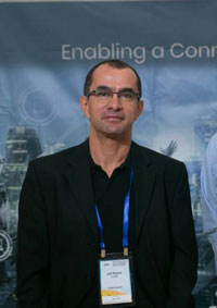
 Meet Iyad Rayane, an experienced Application Engineer in the area of 3D advanced IC packaging and co-design. He recently took the time to chat about his projects at Zuken.
I started my career at a French startup in the Grenoble area specializing in microelectromechanical systems (MEMS). Back then I was a product manager of their CAD tool dedicated to MEMS design. Since then, I have filled different positions with ST Microelectronics and Mentor Graphics working mainly on System-on-Chip (SoC) implementation.
In 2016, I joined Zuken to work on the co-design flow for chips and packaging. Thanks to my background in SoC implementation, I am well-rooted in this type of design flow which enables me to close the gap between the SoC design and the IC package using the co-design flow in CR-8000. Only by understanding both sides, you can draw a complete picture of the overall system and perform the optimization taking into account the constraints from the perspective of the overall system.
Naturally, this led me to work on the systems engineering design flow based on Model-Based Systems Engineering (MBSE) after Zuken acquired the Vitech. The acquisition expands our solution portfolio to include systems engineering, an area of increasing importance to product development companies.
My typical day
I usually work from home, while traveling regularly between different Zuken sites and customer sites. During the pandemic, my typical day is 100 % work from home but filled with plenty of virtual interactions with colleagues in different locations across Europe and Japan.
In addition to the professional side, I also appreciate the cultural side at Zuken, which has allowed me to enrich my personal experiences beyond my day-to-day job.
Break-through Benchmark
One project that stands out for me was one where a customer with unprecedented requirements started a benchmark to replace a competing tool. After intensive collaboration with R&D, we managed to implement the advanced features and ended up winning the benchmark. It happened to be the first customer to adopt the tool and opened the door for many more great adventures.
Peaks and Hummus
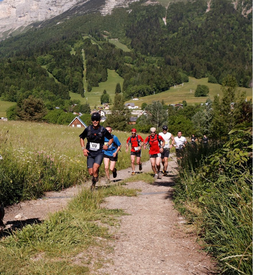
I live in the French Alps surrounded by mountains. Wherever you look, there is a peak to climb. So outside of work, it is the mountains that inspire me. Whether it is winter or summer, there is always a fun activity to do in the mountains. I am a fan of swimming and trail running, exploring the mountains one trail at a time. When the weather is miserable, I practice my second hobby, cooking – needless to say, how delicious my homemade hummus is.
- Products
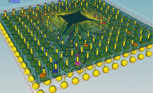
Zusätzlich zum Multi-Board PCB Design unterstützt Design Force auch die Entwicklung von IC Packages für Wire-Bond, Flip-Chip und High-Density Advanced Packaging
- Blog
Advanced packaging techniques such as system-in-package (SiP), fan-out wafer-level packaging (FOWLP), 3D die stacks, etc. have been around for over a decade, yet with any other EDA design tool, it is still a tedious, time consuming, and error-prone process to implement these designs.

