Return Vias, Build-Up Layers and the Latest FPGAs to Battle Latest Signal Integrity Challenges
In the final installment of this blog series, you can learn how to use build-up layers and premium FPGAs to deal with the signal integrity challenges arising from high-speed signals in a 3D design capture world.
Placing return vias
 Luckily, where signals need return vias, component vendors often do most of the work for you. Let’s look at a PCI Express differential pair. First, the standard connector, showing its pinout but not its body; I’ll cover the connector body in a moment. The signal pin assignments are also standardized.
This one is a through-pin component. The two sides of the differential pair (I’ve marked them P and N), are close to ground pins. There’s some differential coupling between the P and N pins and the ground pins create returns in the Z dimension, just like ground planes do for traces.
The connector body works in a similar way. Here’s a small area of the connector, mounted on its footprint. Inside the body, the differential pair has ground metal each side.
 So you can already route this pair from BGA to connector on, say, top and bottom layers, without adding any other vias. If you really need another layer change for a signal like this, then you have to decide on signal via-to-via and return via spacing.
Or do you?
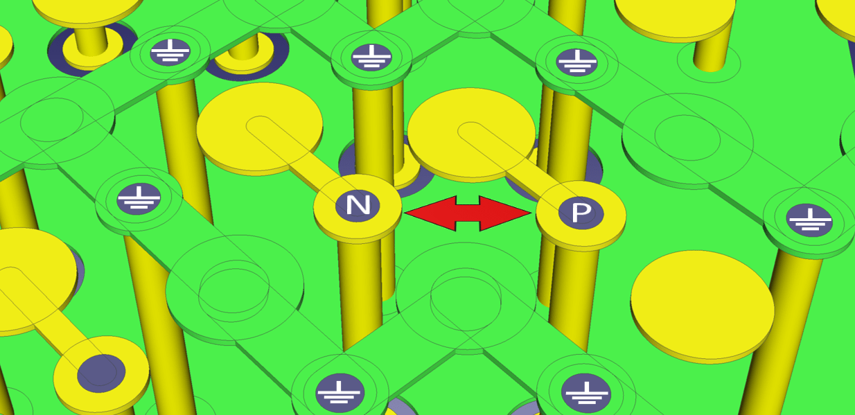
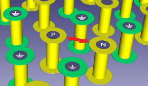
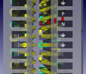
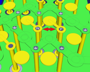
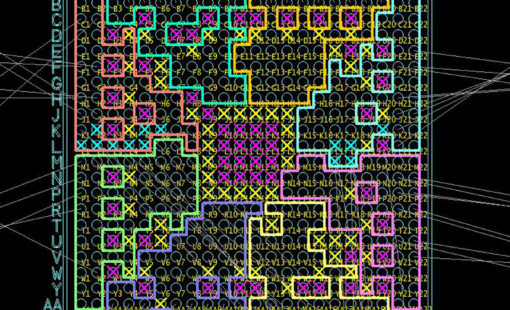
Let’s look at the BGA itself. In this case, its balls are on a 1mm grid, fanned out to vias at even spacing. I’ve added markers on the vias to show the differential pair (N and P) and surrounding ground vias. These signals are on a special high-speed transceiver bank on the FPGA. If you need another layer change, then one way to decide on spacing is just to copy this pattern.
Alternatives to return vias
 You can’t backdrill vias inside the area of a BGA like this, so the alternatives are blind vias or build-up layers. In any case, you often need build-up layers to achieve the high route density that BGAs like this demand. All that’s required then is to restrict routing layers.
- Build-up vias are also much smaller than conventionally-drilled vias and their correspondingly smaller parasitic resistance, capacitance and inductance yield better performance even on slower signals.
- Blind and buried vias add process steps and expense.
- Backdrilling is mainly suited to larger via geometries, so its use is limited, but it’s effective for signals that are a little less critical than PCI Express, such as some SDRAM buses.
Conclusion
Premium components like the FPGA mentioned here include features to help signals fly true. Some of the latest BGA footprints are so fine-pitched that many signals connect through via-in-pad to inner layers only with no room for tracks between pads.
Now that EDA environments work in three dimensions and with high levels of detail, it’s much easier to visualize where signals are going and what will help or hinder them.
Also See:

-
Electronic Design Technology Partner


- Blog
High-Speed-Serial-Links wirken oft wie schwarze Magie – steigende Datenraten verstärken dieses Gefühl. Donald Telian (SI Guys) und Ralf Brüning holen die Diskussion zurück zu den Grundlagen.
- Blog
Lerne die beiden wichtigsten Grundlagen für den zuverlässigen Entwurf von High Speed Serial Links und erfahre, wie du Herausforderungen bei der Signalintegrität bei Geschwindigkeiten von mehreren Gbit/s meistern kannst.

- Blog
CR-8000 2025 integrates AI to support constraint-driven PCB design - offering layout guidance, reusable knowledge, and schematic consistency without removing the engineer from the loop.

- Blog
Die Leiterplattenindustrie entwickelt sich ständig weiter, da technologische Fortschritte und neue Marktanforderungen die Grenzen des Machbaren immer weiter verschieben. Bis 2025 werden mehrere wichtige Trends die Branche prägen. Mehr erfahren? Jetzt in unserem Blog nachlesen!
- Products
Der Graphical Pin Manager von CR-8000 bietet eine effektive FPGA/PCB Co-Design-Umgebung für die neuesten Bauelemente von Anbietern wie Xilinx, Intel, Lattice und Microsemi.
- Products
CR-8000 umfasst eine Suite von Anwendungen, die den gesamten Lebenszyklus des PCB Engineerings abdecken.