Tech-Tip: 2-Re-use Blocks in System Planner
Menu
Believe it or not, you can use your Circuit Block Library for architectural planning too!
Traditional wisdom dictates that a circuit block library can only be used for detail circuit design. The truth is that the proper toolset and solid creative thinking will also give you the same productivity boost, product reliability, and cost benefits at the architectural planning phase too.
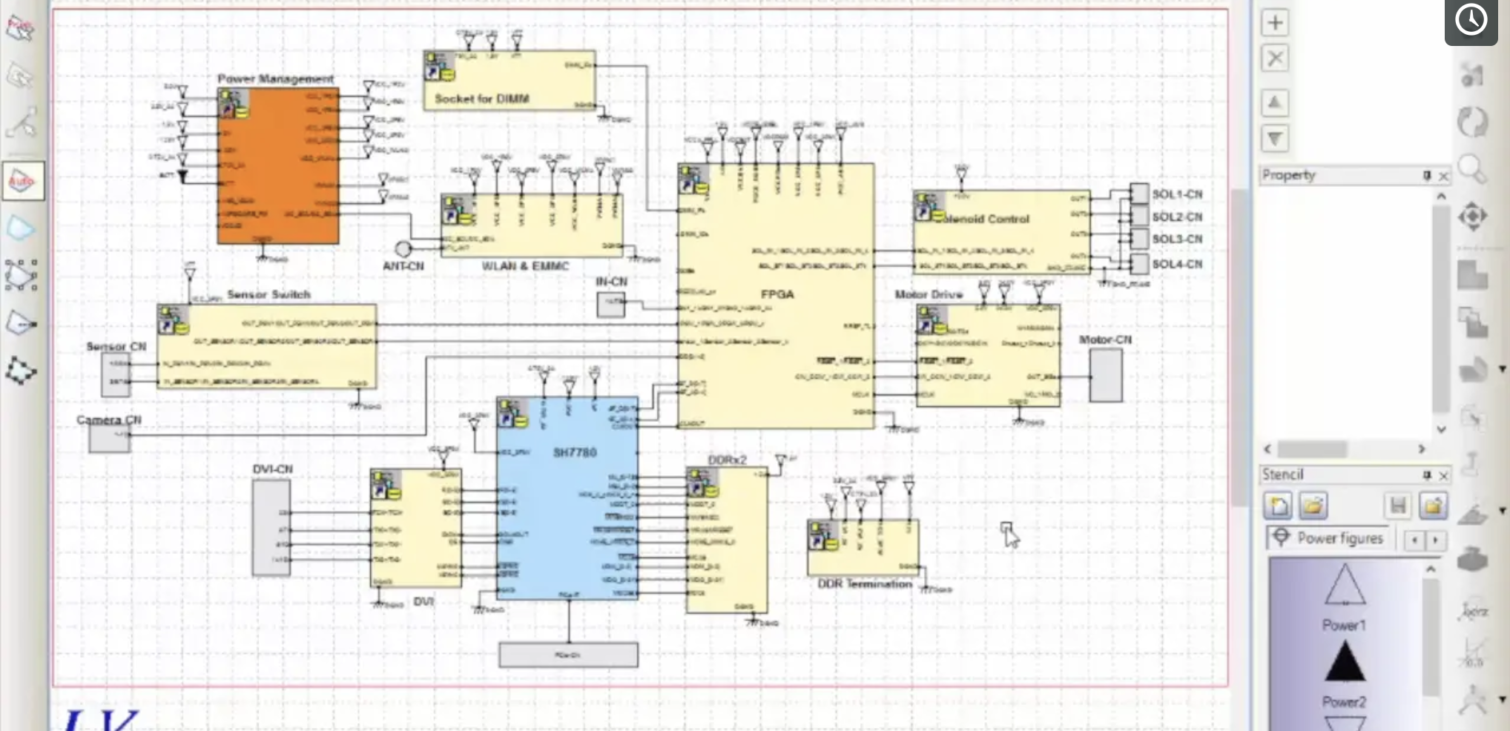
Developing electronic sub-system architectures
The odds are that several to many of the functions you need have already been designed and the ability to tie these sub-system functions to the appropriate logical modules is key to making this happen.
- Access to the same circuit block library that is used by detail design engineering is an absolute must.
- The library needs to be managed:
- Approval control
- Read/write access control
- Easily searchable
- Your architectural planning tool needs to understand the linkage between the function and logical module.
- You need the ability to directly interrogate each logical module for signal interconnects.
- The ability to export a “start point” schematic is a huge advantage.
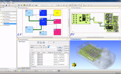
The video that follows will walk you through:
- How to create a functional block and link it to a circuit block module in the library.
- Interconnecting signals between functional blocks.
- Exporting hierarchical and flat “start point” schematics.
Remember to stay tuned to the Zuken Blog! There is more to come on a similar topic.

-
Senior Technical Fellow

Shawn Larson is one of the technical leads for DS product line working primarily on data management implementations. He helps customers to get the right design data in the right place at the right time. Shawn enjoys good jazz, classic rock and all seasons in New Hampshire's White Mountains.

- Blog
Juli 08, 2025
AI in PCB Design: From Misconception to Meaningful Assistance
CR-8000 2025 integrates AI to support constraint-driven PCB design - offering layout guidance, reusable knowledge, and schematic consistency without removing the engineer from the loop.
Read now

- Blog
Januar 31, 2025
Die wichtigsten PCB-Design-Trends für 2025
Die Leiterplattenindustrie entwickelt sich ständig weiter, da technologische Fortschritte und neue Marktanforderungen die Grenzen des Machbaren immer weiter verschieben. Bis 2025 werden mehrere wichtige Trends die Branche prägen. Mehr erfahren? Jetzt in unserem Blog nachlesen!
Read now

- Blog
Januar 23, 2025
Supply Chain Risk Management in PCB Design with SiliconExpert and CR-8000 Integration
Supply chain risk management is critical for electronics design. By integrating SiliconExpert with CR-8000, engineers gain tools to streamline component selection, manage obsolescence, and ensure design continuity. This integration supports efficient workflows, reduces costs, and mitigates supply chain disruptions.
Read now

- Blog
Dezember 05, 2024
Die Zukunft gestalten: Herausforderungen und Innovationen im IoT der Industrie
Von der Automatisierung bis zur Echtzeitanalyse – das Industrial Internet of Things (IIoT) verändert die Industrie grundlegend. Doch hinter den Chancen lauern Herausforderungen: Können Sicherheit, Altgeräte und komplexe Systeme in Einklang gebracht werden? Erfahren Sie, wie intelligente Fabriken der Zukunft gestaltet werden und warum das IIoT der Schlüssel dazu ist.
Read now
Related Content
- Products
Oktober 01, 2018
System Planner
System Planner ist das erste Werkzeug, das ein vollständiges Architekturkonzept von Elektronikprodukten unterstützt. Bislang getrennte Schritte werden intelligent in einer einzigen Applikation zusammengeführt.
Read now
Architekturkonzeption und Validierung

- Products
September 26, 2018
CR-8000
CR-8000 umfasst eine Suite von Anwendungen, die den gesamten Lebenszyklus des PCB Engineerings abdecken.
Read now
Multiboard-PCB-Designsoftware für Fortgeschrittene
- Datenblatt
März 06, 2017
CR-8000 System Planner
Datenblatt, System Planner