Tech Tip: Using Inhibit Layers to Clear Trace Patterns
Menu
In this tech tip, we will explore how you can clear a routed trace pattern on multiple conductive layers.
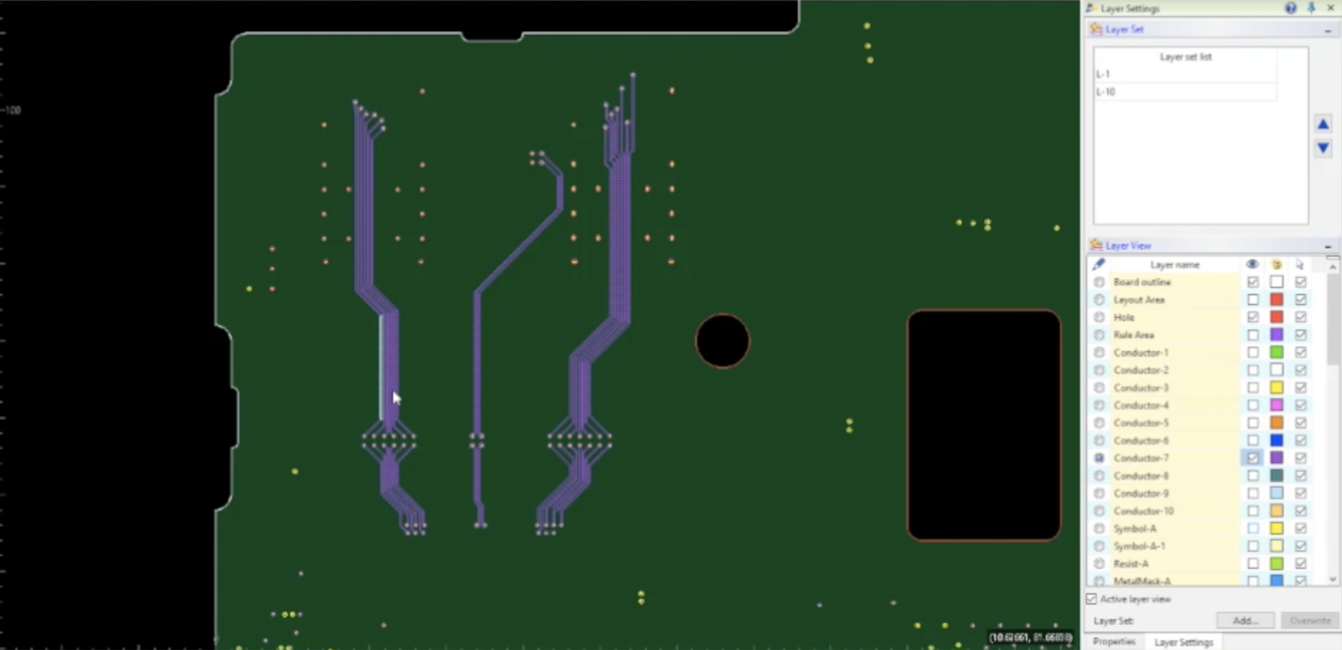
In this design, the requirement is to have these traces on layer 7 to be cleared in the exact same pattern on the conductive areas which are poured on layers 6, 7 and 8.
In this completed example you will see we have these traces routed and they have been cleared on the plane on layer 7. Also, take note that the routed traces have clearances defined on layers 6 and 8.
During today’s tech tip I am going to show you how it’s done!
What we will need is an only track keepout inhibit layer defined that are associated with layers 6 and 8. To set this up I will launch the technology editor. First I will create a user-defined layer and call it InhibitTrack_Layers_6_8. Next, I will right click over the new user-defined layer and select associate with the conductive layer. In this next dialog, I will select both layers 6 and 8 and then set the Layer Type to “Only track keepout” and then select Association. Now take note that this layer is associated with layers 6 and 8.
Next, I will set the active layer to InhibitTrack_Layers_6_8 and I will select the Figure tab and select Offset.
Now I will use the Offset function located on the Figure tab of the ribbon.
In the parameters, dialog set the “Mode” to Area Fill and then set the direction to Outside. Then set the offset value to .1. Next, I will frame select the traces and the offset is generated on to InhibitTrack_Layers_6_8
So far so good!

-
Director of Customer Support
Sandy Jones is a Director of Customer Support ensuring customers are well taken care of by guiding her team to achieve support excellence. Her work focuses on improving customer support procedures through regular communication along with managing training activities and materials. In her free time, she enjoys repurposing old barn wood windows by painting images on the glass.

- Blog
Januar 31, 2025
Die wichtigsten PCB-Design-Trends für 2025
Die Leiterplattenindustrie entwickelt sich ständig weiter, da technologische Fortschritte und neue Marktanforderungen die Grenzen des Machbaren immer weiter verschieben. Bis 2025 werden mehrere wichtige Trends die Branche prägen. Mehr erfahren? Jetzt in unserem Blog nachlesen!
Read now

- Blog
Januar 23, 2025
Supply Chain Risk Management in PCB Design with SiliconExpert and CR-8000 Integration
Supply chain risk management is critical for electronics design. By integrating SiliconExpert with CR-8000, engineers gain tools to streamline component selection, manage obsolescence, and ensure design continuity. This integration supports efficient workflows, reduces costs, and mitigates supply chain disruptions.
Read now

- Blog
Dezember 05, 2024
Die Zukunft gestalten: Herausforderungen und Innovationen im IoT der Industrie
Von der Automatisierung bis zur Echtzeitanalyse – das Industrial Internet of Things (IIoT) verändert die Industrie grundlegend. Doch hinter den Chancen lauern Herausforderungen: Können Sicherheit, Altgeräte und komplexe Systeme in Einklang gebracht werden? Erfahren Sie, wie intelligente Fabriken der Zukunft gestaltet werden und warum das IIoT der Schlüssel dazu ist.
Read now

- Blog
November 28, 2024
Stack-Up Design und Impedanzkontrolle für High-Speed Leiterplatten
Der Layer-Stack-up und die präzise Berücksichtigung der Leitungsimpedanz sind entscheidend für robuste High-Speed-Designs. Erfahren Sie in unserem Blog, wie Sie Stack-ups optimal mit CR-8000 und Polar Speedstack™ gestalten können.
Read now