
Zuken Supports Next-Generation 3D LSI-Semiconductor Mounting Design Technology
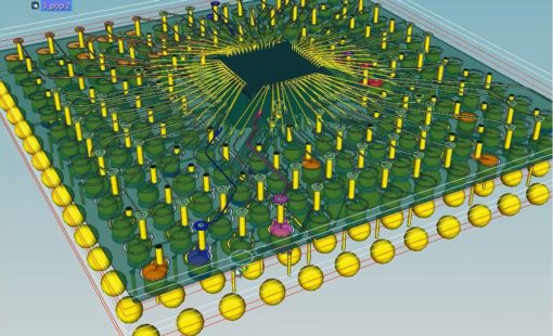
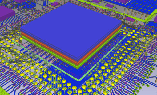
With the utilization of CR-8000 Design Force, Zuken helps to overcome design challenges associated with 3D integration in the pursuit of next-generation semiconductor technologies.
Munich, Germany, and Westford, MA, USA, December 6, 2022 – Zuken has established a partnership with the WOW Alliance headed by Professor Takayuki Ohba from the Research of Science and Technology Laboratory at the Tokyo Institute of Technology. The WOW Alliance is an industry-academia research platform that brings together various stakeholders, including companies, universities, and research institutions, with the goal of advancing the development of next-generation semiconductors using wafer-on-wafer (WOW) integration technologies.
Led by the Laboratory for Research and Technology at the Tokyo Institute of Technology, the WOW Alliance is actively involved in the advancement of a cutting-edge chiplet integration technology. The primary focus of the Alliance is to tackle the challenges associated with 3D integration, encompassing concerns such as power consumption, thermal resistance, and performance enhancement with a comprehensive solution that not only addresses these challenges but also delivers enhanced overall performance in semiconductor systems.
As a result of its joint effort with industry and research partners, the WOW Alliance has developed a proprietary wafer thinning technology to address the limitations of conventional wafer thickness, reducing it from the typical range of 20-30 μm to an ultra-thin 4 μm. Moreover, the alliance has also implemented a bump-less Through-Silicon Via (TSV) interconnect technology, eliminating the need for traditional bumps. Additionally, terabyte-level high bandwidth transmission is achieved through high-density super parallel interconnects, enabling the stacking of wafers in the WOW (wafer on wafer) and COW (chip on wafer) configurations.
To support the design requirements of the new technology, Zuken contributes its CR-8000 Design Force multi-board design environment. This powerful design tool enables the alliance to effectively tackle the complexities of 3D integration and facilitate the design process for integrated circuits.
For more information, please visit WOW Alliance | Takayuki Ohba Laboratory, Laboratory for Future Interdisciplinary Research of Science and Technology, Tokyo Institute of Technology (titech.ac.jp)
About the WOW Alliance
Semiconductors for CPUs and memory, indispensable for personal computers and smartphones, have improved performance through device shrinkage. However, the industry is currently facing the inherent physical constraints of conventional technology when it comes to further reducing the size of semiconductor components.
To overcome these constraints, the WOW Alliance lead by the Laboratory for Future Interdisciplinary Research is developing a three-dimensional large-scale integration (3D LSI) technology using vertical interconnect technology and special ultra-thinning technology for semiconductor die stacks that is capable of improving performance while making the stacks smaller and thinner.
Using this technology, the members of the WOW Alliance are working to integrate multiple semiconductor functions into a one-stack module, surpassing the limits of shrinking devices in two-dimensions only. For more information, please visit WOW Alliance | Takayuki Ohba Laboratory, Laboratory for Future Interdisciplinary Research of Science and Technology, Tokyo Institute of Technology (titech.ac.jp)
- Presse-Information
Zuken Inc. today announced that it has joined the EDA Alliance in TSMC’s Open Innovation Platform® (OIP). TSMC collaborates with its OIP EDA Alliance partners to address growing design demands, accelerate adoption of latest process and packaging technologies, and enable customers to achieve their PPA and time-to market targets.
- Presse-Information
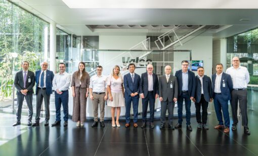
Valeo and Zuken are partnering through the Zuken Valeo InnoLab to create an open, AI-assisted electronic design platform for automotive engineering. The collaboration combines Zuken’s AI architecture with Valeo’s AI Agents and industrial expertise to reduce design times, strengthen digital continuity, and support robust electronic design across the full design flow.
- Blog
Modern electronic products are no longer built around a single PCB. As systems become faster, denser, and more interconnected, engineering teams are being forced to rethink how they design, verify, and manage complex multi-board products.
- Blog
Explore how CR-8000 enhances PCB design with integrated control of impedance and resistance—enabling precise analysis for both high-speed and high-power applications, from signal integrity to power distribution optimization.
Related Content
- Products
Zusätzlich zum Multi-Board PCB Design unterstützt Design Force auch die Entwicklung von IC Packages für Wire-Bond, Flip-Chip und High-Density Advanced Packaging
- Products
Zusätzlich zu den hochentwickelten Funktionen für das PCB-Layout bietet Design Force die Möglichkeit des Co-Designs von Chips, Gehäusen und Leiterplatten, so dass ein hierarchisches 3D-Design in Echtzeit ermöglicht wird.