- Blog
Well, there’s no doubt about it: Developing circuit boards is getting more complex. Demand for faster data speeds is increasing. Boards are becoming more dense. Requirements call for the latest protocols and devices. Packaging constraints call for multi-board and flex-board systems. The surest sign of escalating board complexity lies in the fact that few are designed by a single engineer. Today, most require the coordination of many engineers instead. And overall, this trend shows no sign of abating. Board complexity looks like it will only get worse...

- Blog
PCB designers working with advanced and complex designs are constantly pushing the boundaries to satisfy the signal integrity of routed differential pairs and busses. Those who work with flexible and flex-rigid PCB designs are perhaps the most demanding of all. A while ago, the introduction of the curved corner style for routing trunks in CADSTAR made a big difference to this group of users.

- Blog
It sounds like a paradox: electronics manufacturers can increase variation within a product line while using fewer electronic components. Reuse keeps product costs low, increases product flexibility and customization. Far from paradoxical, the approach is quite doable today through a process called modular board design coupled with predictive analysis numbers returned by the Internet of Things.

- Blog
It has often been noted that many of the aircraft and other weapons systems used by the armed forces are older than the service men and women operating and maintaining them. While the average age of a U.S. domestic commercial airliner is 11 years, it is not uncommon for aircraft to still be in service at 30 years. Likewise, there are many machines and systems in electric power generation, discrete parts manufacturing, chemical process, oil and gas production and many other industries that have been in continuous operation for several decades or longer.

- Blog
Japan is one of the first countries to face the combination of challenges such as energy issues, population decline and an aging society. Solving these problems with the benefit of the Internet of Things (IoT) could generate future business opportunities as well as meeting the demands of society. Enabling as many people as possible to try out new ideas, and encouraging them to develop diverse products, will broaden these opportunities. The Trillion-Node Engine is a platform for realizing this objective.

- Blog
Take a walk in the engineer’s shoes: I need an 80 MHZ network controller for my new project and I found one in the PLM/PDM system. That was easy. Now a quick check in the procurement database to do a price and availability check. So far so good, now on to the component engineering system to see if there are any possible lifecycle issues with a 10-year minimum requirement. It’s my lucky day, no issues and it’s a company-preferred part with an ECAD library instance.

- Blog
Using feedback from products in the field to continuously improve design modules used as the basis for product development can increase product performance and reliability and reduce development time.

- Blog
As we welcome increasing numbers of IoT devices into our industries, offices and home lives, we shouldn’t be surprised to see increasing electromagnetic (EM) congestion. Or, as it’s now dubbed, the ‘Interference of Things’.

- Blog
A customer recently asked me if CR-8000 Design Force could support stretchable flex designs. At first, I found the question odd, until they shared their intent: wearable electronics. The idea of wearable electronic products like head and wrist bands sparked an interesting conversation and piqued my interest.

- Blog
Man-carried military communication systems often consume large amounts of power. The heat must be removed from the electronics package to avoid frying sensitive electronic components. The package typically is designed to be carried in a backpack which often puts difficult constraints on the form factor and weight of the system

- Blog
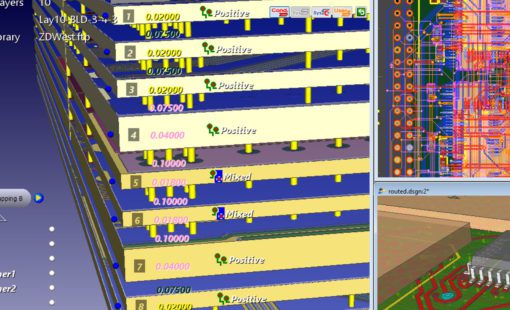
We’re happy to announce that Speedstack, Polar Instruments’ layer stackup design/documentation tools, can now be directly linked to Zuken’s CR-8000 Design Force and DFM Center.

- Blog
Tips for when routing differential pairs - You can tell when something isn’t as clear as it should be. The same questions come up time and again. You ask three experts and get three different answers. Routing differential pairs can be like that. Why? Because “it depends” - on exactly what signals those pairs are carrying and what kind of PCB you’re creating.

- Blog
Do you still use Post-it Notes? Invented in 1979, this simple, yet incredibly powerful, communication mechanism is still commonly found in engineering and design departments. Despite modern electronic communication, many companies still struggle to provide a replacement for their ease-of-use and versatility.

- Blog
Zuken has been developing PCB design tools for the automotive market for years. With automotive electronics worth over $200 billion globally, and growing every day, Zuken is preparing for a brave new world of smart cars, and autonomous and electric vehicles.

- Blog
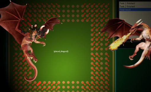
Simply draw a Dragon area around your BGA. Then select the Dragon area and create a strategy to fanout the pads of your BGA - Watch movie

- Blog
There is one thing that all design engineers will agree on: creating and gathering all the required data for PLM is error-prone and can be a royal pain. We all understand the value of releasing our design data to the corporate PLM system but our design process dictates multiple release points, and each one has a different purpose and data requirements.