The design of DDR4 (Double Data Rate 4) defines, like many other high-speed applications, the quest to allow transmitting large amounts of data at the highest possible speed between a driver (CPU/FPGA) and one or multiple receivers (DRAMs). DDR was introduced in 1998 and has continued to evolve ever since. Subsequent generations include DDR2 (2003), DDR3 (2007), and DDR4 (2014). DDR5 has been introduced in 2021 and DDR6 is expected for 2024.
Although the technology continues to evolve towards DDR5 and DDR6, in the current technology landscape, DDR4 (and its low power version LPDDR4) is often a critical hurdle in the design process of an electronic application because of the large number of rules and constraints which have to be obeyed for the implementation of high-performance memory subsystems.
DDR3 vs. DDR4 – what’s the main difference?
While the architectural concepts (routing topology in a daisy chain fly-by bus) have not fundamentally changed from previous generations, the design of DDR4 systems is somewhat more challenging than the previous versions. DDR4 data rates are now twice as fast as DDR3 due to improvements in the on-chip pre-fetch technology and the new Data Bus Inversion (DBI) technology, but DDR4 requires more precise control of length matching and impedance and signal integrity control (sufficient eye openings).
Pre-fetch in DDR systems improves the efficiency of memory access by fetching a larger block of data, called a pre-fetch buffer or burst, before it is specifically requested. This predictive approach helps to overcome memory latency by allowing the memory controller to overlap operations and fetch the next set of data into the pre-fetch buffer while the current data is being transferred to the CPU (Source: Wikipedia).
With the newly added DBI signals, the DDR4 controller monitors the number of 0s and 1s in each byte of the transmitted information. Normally, a 1 represents a high level and a 0 a low level. If there are more 0s than 1s, the controller inverts the data and sends out a signal indicating that the data is inverted. This minimizes the load on the memory bus as never more than half is grounded, and results in a reduction of power surge by a factor of two (It may be important to note that this is a property of the DRAM interface, not for the whole board).
Routing of DDR4 Systems
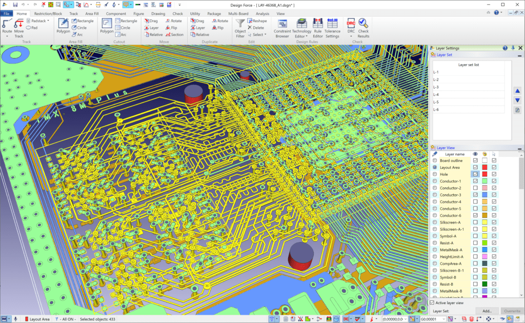
In addition, DDR4 allows for higher density memory modules, which poses severe routing challenges. Managing the higher density without compromising performance or stability requires advanced PCB design techniques to adhere to the following fundamental rules:
- Data byte-lane members should be routed on the same layer majority of routing path, stripline highly recommended).
- Address/command/control/differential clocks net groups should be routed on the same layer (if possible, if space issues occur, they may be separated onto different layers but try to keep the groups together). Maintain the electrical (!) skew requirements for these groups.
- Adjacent layers or layers referencing the same plane layer are preferred.
- If you use more than one DRAN, then address/command/control/differential locks route topology to be routed using daisy chain (fly-by) technology (as not all memory controllers support Y/T topologies), then route from controller starting with chip 0 through chip n in order by the byte-lane numbers.
- Maintain the holy rule of EMC compliant PCB-routing – never route any of these signals over a split/gap on the reference plane.
Moreover, the operational voltage of DDR4 is reduced to 1.2 volts comparing to the 1.5 volts used by DDR3. This reduction in voltage is a significant contributor to improved energy efficiency, a crucial factor in contemporary electronics aiming for lower power consumption and extended battery life in portable devices. However, this shift to lower voltage levels introduces challenges related to signal and power integrity. As the voltage decreases, the signals become more susceptible to noise, attenuation, and other factors that can affect their quality.

DDR4 Design Considerations
Maintaining signal integrity becomes a critical aspect of DDR4 design, requiring careful consideration of factors such as impedance and skew matching, signal termination, and advanced PCB layout techniques to ensure reliable communication and optimal performance in the face of reduced voltage levels. The trade-off between energy efficiency and signal integrity underscores the complexity and careful balancing act involved in DDR4 system design.
DDR4 design is challenging but not rocket science, it requires definitely a certain amount of diligence and care during development. Our webinar library offers you the opportunity to dive deeper into the world of high-speed PCB Design. Learn everything from best practices to advanced techniques to achieve optimal system performance.
To read more on Zuken’s high-speed pcb design solutions please see Design Force Signal Integrity Advance. This new, comprehensive bundle within the CR-8000 Design Suite covers all aspects of Signal Integrity from Characteristic Impedance to IBIS AMI analysis of SerDes channels.

- Webinar
In this presentation you will be introduced to the necessary steps in constraining and validation of LPDDR4 on the basis of a real design realized in CR-8000 Design Force right first time.

- Software Evaluation
CR-8000 is a suite of applications that span the entire PCB engineering lifecycle: from architecture planning through system level engineering and optimization, to physical 2D/3D implementation and manufacturing outputs. Includes; Design Force and Design Gateway, plus any other CR-8000 module you specify.


