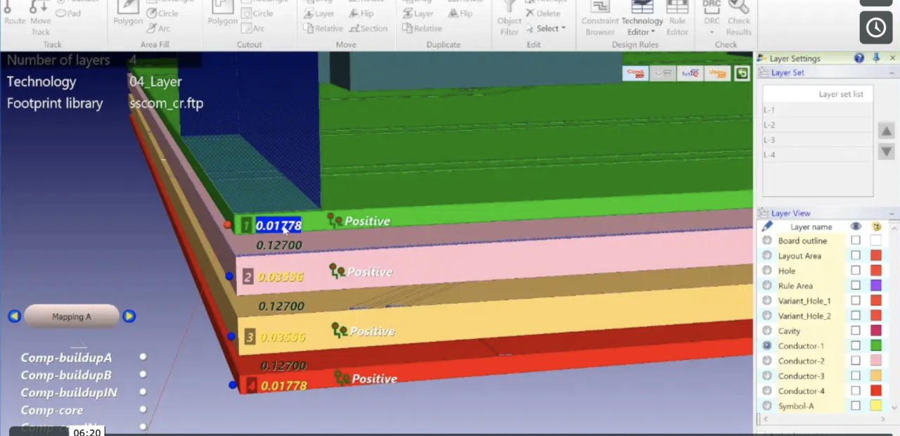
Tech Tip: Design Force 3D Technology Editor
In Design Force you can edit your board Technology using the 3D Technology Editor. In the 3D technology edit window, you can perform the following operations to edit the technology for the board.
“Adding or Deleting a Conductor Layer to/from a Board (3D)”
“Adding or Deleting a User Defined Layer to/from a Board (3D)”
“Editing Layer Attributes of a Board (3D)”
“Editing the Layer Mapping of a Board (3D)”
In the video, I also use the 2D Technology Editor to edit the displayed layer order and comments. I also edit the board configuration in the Rule Editor to make sure my design is ready for the simulation tools.

-
Applications Engineer


- Blog

- Blog
Modern electronic products are no longer built around a single PCB. As systems become faster, denser, and more interconnected, engineering teams are being forced to rethink how they design, verify, and manage complex multi-board products.

- Blog
Explore how CR-8000 enhances PCB design with integrated control of impedance and resistance—enabling precise analysis for both high-speed and high-power applications, from signal integrity to power distribution optimization.

- Blog
Related Content
- Products
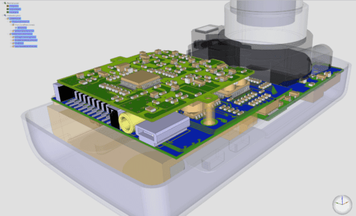
CR-8000 Design Force is the fastest, most effective PCB design solution available today. Design Force enables design teams to layout and verify their designs in the context of a complete system or product.

- Products
CR-8000 is a System-Level PCB & IC Package Design software including 3D Multi-board, Analysis and MCAD Integration