
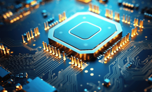
Exploring the Essentials of High-Speed PCB Design
Explore the world of high-speed PCB design, where impedance control and signal integrity ensure top-notch reliability.
Menu
In the world of advanced electronics, high-speed PCBs are the unsung heroes that enable our modern devices to perform their magic. These typically hidden circuit boards play a pivotal role in ensuring that signals flow seamlessly. Now, let’s take a journey through the essential aspects of high-speed PCB layout, with each aspect serving as a gateway to deeper knowledge.
High-Speed PCB Design – The Silent Workhorse for Engineers and Product Designers
As technology emerges, PCB design faces new challenges that make it increasingly complex and demanding. In the dynamic field of electronic engineering, the intricacies of PCB design are being continually reshaped by technological progress. Designers now grapple with crafting smaller, more powerful, and energy-efficient electronic products. This quest for innovation requires a delicate balance of elevating performance standards while judiciously managing expenditures. Compounding these challenges is the accelerating pace of design cycles, demanding rapid yet effective decision-making in PCB design processes.
Additionally, optimizing routing is crucial to reduce signal losses, and engineers must also grapple with the increasing power demands of modern ICs. To make life even more complicated for the designer, observation of advanced manufacturing processes is essential to maximize yield without compromising quality. Curious to know more about the evolving landscape of PCB design? Explore our article “Mastering the Challenges of Modern PCB Design” to gain insights into the dynamic world of electronic design.
Key Parameters for High-Speed PCB Design
Signal integrity performance and impedance control represent the higher ordinations in high-speed PCB layout. These aspects are crucial to guarantee the reliability of your electronic devices. They work together seamlessly to ensure the smooth flow of data through your circuits.
-
Impedance Control
Impedance control is all about fine-tuning the parameters of signal pathways. It plays a critical role in ensuring that signals propagate optimally throughout the PCB. Impedance mismatches (‘discontinuities’) will create reflection points (voltage dividers) yielding increased noise. For a comprehensive understanding of the topic, I recommend diving into our guide on “Signal Integrity Basics: Impedance Control”.
Learn More About Impedance Control
-
Signal Integrity
Signal integrity is responsible for the smooth and reliable transmission of data within PCB circuits. It acts as a critical safeguard, ensuring that signals travel without disruption. There are various aspects to consider, just to name a few: reflection, ringing, crosstalk, propagation delay, electrical skew, insertion loss, and return loss. If you’re interested in exploring how CR-8000 Design Force can assist you in mastering signal integrity, visit our CR-8000 Design Force page.
Together, signal integrity and impedance control ensure that your high-speed PCBs perform at their best. They deliver the quality and reliability expected in modern electronics.
Power Distribution Network: The Energy Hub
The Power Distribution Network (PDN) acts as the energy hub in high-speed PCBs, guaranteeing stable and efficient power distribution across electronic devices. It’s comparable to the circulatory system in our bodies, ensuring every component receives the energy it requires. The choice of materials and layer stack-up is fundamental. Delve deeper into the world of materials and layer stack-up in our article, ” What PDN Target Impedance Means for PCB Designers“. It will help you understand how these choices impact your PCB’s performance.
Conclusion: Elevate Your High-Speed PCB Design with CR-8000
Mastery of high-speed PCB design demands a multi-faceted approach. This includes meticulous planning and material selection, along with complex simulations and robust testing. Fortunately, CR-8000 embodies all these essential features, making it an indispensable tool for engineers and product designers. By leveraging the capabilities of CR-8000, you can turn your high-speed PCB designs into paragons of efficiency and reliability.

Ralf works as Product Manager for High-speed Design Systems at the Zuken EMC Technology Center in Paderborn/Germany, responsible for product marketing and business development for the Zuken SI, PI and EMC analysis tools. He holds a diploma degree in computer science, electrical engineering and economics from the University of Paderborn. He has 30 years of experience in Electronics and EDA. He is regular speaker on international conferences, but is involved in European Funding project and standardization activities as well.
- Blog
September 13, 2023
Mastering the Challenges of Modern PCB Design
Printed Circuit Board design has been at the core of electronic innovation for decades. However, as technology continues to advance, PCB design faces new challenges that make it increasingly complex and demanding.
Read now
- Blog
September 20, 2021
What PDN Target Impedance Means for PCB Designers
PDN impedance is becoming more and more of a headache for PCB designers as IC vendors are defining increasingly tight so-called ‘target impedance limits’. This article explains what PDN impedance means for PCB designers and what to pay particular attention to.
Read now

- Blog
February 21, 2019
Inside Signal Integrity: Impedance Control - Part 1
Impedance and impedance control are some of the oldest and most discussed topics in PCB design. They are especially important in high-speed design related to signal integrity. In this, the first of a two-part blog, we’ll go back to the basics of impedance/impedance control and consider what influences line impedance. In part two, we’ll set about controlling it.
Read now
- Blog
September 13, 2023
Mastering the Challenges of Modern PCB Design
Printed Circuit Board design has been at the core of electronic innovation for decades. However, as technology continues to advance, PCB design faces new challenges that make it increasingly complex and demanding.
Read now
- Blog
September 20, 2021
What PDN Target Impedance Means for PCB Designers
PDN impedance is becoming more and more of a headache for PCB designers as IC vendors are defining increasingly tight so-called ‘target impedance limits’. This article explains what PDN impedance means for PCB designers and what to pay particular attention to.
Read now
- Blog
February 21, 2019
Inside Signal Integrity: Impedance Control - Part 1
Impedance and impedance control are some of the oldest and most discussed topics in PCB design. They are especially important in high-speed design related to signal integrity. In this, the first of a two-part blog, we’ll go back to the basics of impedance/impedance control and consider what influences line impedance. In part two, we’ll set about controlling it.
Read now