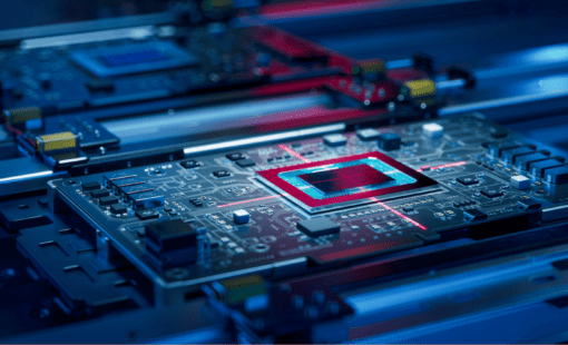
Harnessing the Power of Artificial Intelligence for PCB Design
With the release of ChatGPT at the beginning of the last year, artificial intelligence, or AI for short, has become a topic that has stirred many emotions. The reaction to the first encounter with an AI tool can be compared to seeing a circus horse that can do math: You are amazed and wonder how this can work? It has to be some sort of a trick!
The optimists among us immediately started thinking ahead, figuring out how to use the new technology to delegate tedious tasks such as composing emails, press releases, website content, or even essays and university theses to an AI tool while enjoying the finer things in life. The more pessimistic characters, on the other hand, tended to fear that their jobs would be threatened Both reactions are probably not entirely unjustified. But that is not the subject of our discussion today.
Is AI suitable for complex engineering tasks?
Instead, we want to explore whether AI could one day be used to support Zuken’s core business of solving complex design challenges such as PCB layout and routing. Part of the answer – spoiler alert! – is yes, it can, but it’s not as simple as you might think. Something like: take a connection list and the corresponding list of components and feed it into an AI engine; add a few boundary conditions such as PCB contour, drill holes and cut-outs and the number of permissible layers and – voilà – you get a fully placed and routed PCB layout.
So let’s ask a man who has been working on the use of artificial intelligence in PCB design for some time, and who recently introduced the first version of AI-powered PCB design software: Dr. Kyle Miller, Research and Development Manager at Zuken Technical Center, Bristol. Kyle is responsible for developing automation routines for PCB layout and routing and has been involved with AI since his student days.
Using AI is all about balancing creativity, accuracy, and precision
“The main problem with the AI tools available today is reconciling the conflicting aspects of creativity, accuracy, and precision,” he says, referring to a circuit diagram he created using an AI-based image generator. It shows a diagram that looks very similar to a circuit diagram on the surface, but is somewhat meaningless in detail. “It is a reasonably accurate representation of a schematic, but it lacks precision.
And he continues: “If I ask a text generator like ChatGPT, I may get very precise answers, but they may be inaccurate or even wrong. Or I may get a general description of the process, which may even be accurate, but does not provide a useful result. The challenge in PCB design and design applications in general, according to Dr. Miller, is to balance all three aspects, namely creativity, accuracy, and precision.
To learn more about how Zuken approached the task of using AI for PCB design and the methodological considerations Kyle and his team made, watch our webinar, “AI-Based PCB Place and Route is All About Machine Learning”.
PCB design is facing a shortage of skilled engineers, and AI has arisen as a potential solution for bridging this skill gap. Dive deeper into our blog and discover how to “Address the Skill Shortage in PCB Design with AI“.


- Blog
Modern electronic products are no longer built around a single PCB. As systems become faster, denser, and more interconnected, engineering teams are being forced to rethink how they design, verify, and manage complex multi-board products.
- Blog
Explore how CR-8000 enhances PCB design with integrated control of impedance and resistance—enabling precise analysis for both high-speed and high-power applications, from signal integrity to power distribution optimization.

- Blog

- Blog
AI in PCB design is increasingly seen as a game-changer, with some predicting it could soon replace entire layout teams—but this view risks overlooking both the current limits of AI and the critical expertise engineering demands. At DesignCon 2025, experts from emphasized that AI's real value lies in complementing human judgment, not replacing it. Read more on our blog.