A trend towards low power design prevails in the electronics industry today and is not likely to change in the near future. This development is driven by many reasons but primarily by the performance and storage density demands of mobile devices, where a reduction of the power consumption is crucial to extending battery life without sacrificing the bandwidth.
However, low power DDR memory is now spreading to other industries such as industrial automation and the automotive industry as well. Electromobility is seen as the key to climate-friendly mobility and innovation worldwide, but it requires a high level of energy efficiency in all electronic components on board, which ultimately all require energy from the battery. This ongoing trend poses new challenges for PCB designers as data rates exceed multiple giga-transfers per second and timing margins are shrinking further with every memory generation.
High density for small form factors
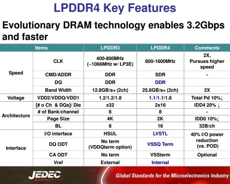
LPDDR, an abbreviation for Low-Power Double Data Rate is a type of memory that operates on a lower supply voltage level (compared to regular double data rate memories) and consumes less power. It was initially targeted for smartphones, tablets, and other smart connected devices that facilitate the industry 4.0 with its cloud applications and big data. In other words, the here discussed LPDDR4 is the mobile equivalent of DDR4 with a higher memory bandwidth and a reduced voltage level and with some minor other functional differences. Interestingly, its share of the total memory market has been growing over the past years, so it’s not unlikely that it will show up in one of your next bill of materials.

What are the challenges in design and validation?
Following the framework of the JEDEC standard JESD209-4C, the relevant rules and constraints for LPDDR4 memory devices and their usage have been adopted by all semiconductor vendors. This led to more stringent design rules for designers using this kind of memory.
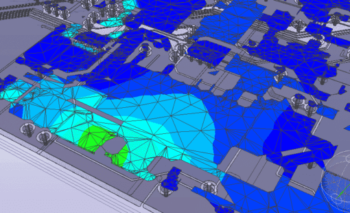
In addition, the form factors of many printed circuit boards are getting smaller and smaller. Therefore, parasitic effects like crosstalk or PDN noise gain importance as trace lines are routed even denser on the board and designers are fighting for every square millimeter and may question every single decoupling capacitor. To add more fuel to the fire, in LPDDR4 design the ICs can be tweaked in a more extensive way compared to DDR3, resulting in many different parameter settings (overshooting, embedded termination devices on driver and receiver side, driving strength and impedance, etc.) that change depending on the design intent. These design challenges are these days quite similar to SERDES in terms of complexity.
Solving LPDDR4 Design Challenges
The tight timing and voltage constraints require a holistic design approach that combines high-speed constraining and integrated analysis techniques to comply with the various design rules. Especially important for design success is a carefully considered pre-layout phase. This should include simulations to find the proper trace width, considerations about the spacing to avoid crosstalk, and calculations to limit the damping and time delay effects of vias in the interconnect path. Careful planning in pre-layout allows design optimization in terms of cost and form factor and to achieve the maximum system performance.
In our on-demand webinar Solving LPDDR4 Design Challenges Ralf Brüning, Product Manager and Senior Consultant for High-Speed Design Solutions, will explain the steps necessary to constrain and validate LPDDR4 using a real-world design that was successfully implemented with CR-8000 Design Force right the first time.

- Webinar
In this presentation you will be introduced to the necessary steps in constraining and validation of LPDDR4 on the basis of a real design realized in CR-8000 Design Force right first time.

- Webinar
In our webinar we will provide an introduction to the challenges of signal integrity and the underlying physical effects. This will provide the basis for practical tips to address the related challenges during PCB design.

- Webinar
In this presentation, an EMC minded PCB design approach is presented, allowing designers to understand which EMC rules will apply to PCB projects and how EMC analysis capabilities can be utilized in the CAD flow to reduce the risk of EMC compliance failure once the board is manufactured.


