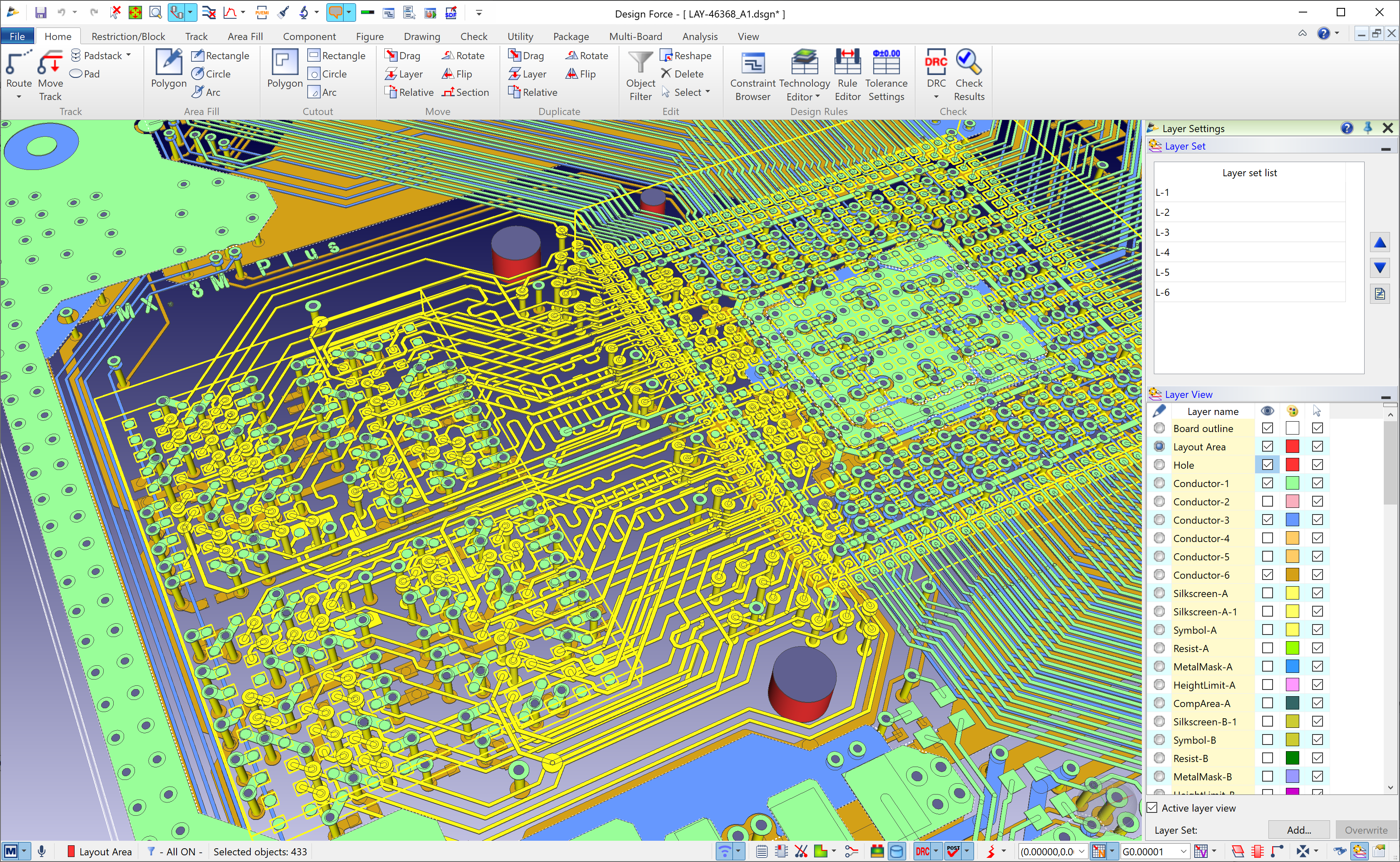
The arrangement of the various layers in a multilayer PCB, commonly referred to as layer stack-up, and careful attention to the electrical impedance of the tracks are crucial factors for achieving robust high-speed board designs. Poor choices in either area can lead to significant performance issues, such as signal loss, electromagnetic interference issues (EMI), and ultimately delays and higher costs due to comprehensive re-design.
Mastering PCB stack-up design and track impedance is therefore essential for creating reliable, high-performance PCBs. By understanding the key factors that influence these design aspects and leveraging the analysis and simulation capabilities of advanced design tools, engineers can significantly improve their boards’ performance and reliability. So, before setting out to actually create a board design, it is good engineering practice to spend some time on key design parameters to avoid pitfalls and enhance the board’s overall performance.
Selecting the Appropriate Materials to Balance Cost and Performance
While FR-4 is the most common PCB material, it has limitations in high-speed applications due to its higher dielectric constant (Dk). Low-loss dielectrics like PTFE laminates, ceramic-filled hydrocarbon materials, or polyimide-based laminates offer superior electrical performance in high-speed and high-frequency applications but are more expensive than standard FR-4. Additionally, they are softer and therefore require specific fabrication methods to avoid deformation during drilling and etching. They are also critical with respect to environmental influences, such as humidity.
Layer Arrangement for EMI Reduction and Crosstalk Control
The order in which signal layers and ground/power planes are arranged directly impacts EMI control and crosstalk. A well-designed stack-up separates high-speed and low-speed signals by placing them on dedicated layers. These in turn should be complemented by dedicated power and ground planes to provide shielding and a stable return path. For example, a typical 4-layer PCB stack-up for balancing power distribution, EMI and crosstalk reduction would be ‘Signal-Ground-Power-Signal’. For more sensitive mixed-signal or analog-digital systems, a more costly ‘Signal-Ground-Ground-Power’ configuration provides excellent EMI shielding, especially for high-speed signals.
Determining the Optimal Copper Thickness
Copper thickness plays a crucial role in the signal integrity of high-speed PCB designs in several ways. Thicker copper in high-speed PCB designs offers both benefits and challenges for signal integrity. On the positive side, it reduces conductor losses by lowering resistance, which minimizes signal attenuation over long distances. It also improves signal propagation by reducing inductance, helping to prevent distortion and delays. On the other hand, thicker copper complicates impedance control, as it requires wider traces that can lead to signal reflections and crosstalk. It also increases the need for larger spacing between traces, complicating routing in dense designs.
To achieve consistent impedance, it’s therefore crucial to calculate and design for the right track width and spacing early in the design phase. Advanced PCB design tools, like CR-8000, come equipped with built-in signal integrity analysis that helps automate and verify impedance control during layout.
Design Tools for PCB Optimization Help Balance Conflicting Requirements
It is obvious that most, if not all the above aspects and requirements are quite conflicting and need a balanced trade-off. State-of-the-art PCB design software like CR-8000 can assist designers in achieving the requested performance metrics with integrated calculation and simulation tools.

CR-8000 offers several advanced features for optimizing PCB designs. It includes integrated signal and power integrity analysis, allowing engineers to simulate and ensure optimal performance across all layers. A stack-up planning feature simplifies layer sequencing and material selection to reduce interference. Additionally, the software provides real-time impedance calculation, automatically checking impedance during track routing to ensure consistency and accuracy, ultimately enhancing signal integrity and reducing design errors.
The Benefits of Perfecting PCB Stack-Up Design
Engineers who master stack-up design and impedance control will see significant improvements in their PCB designs: They will achieve better performance due to improved signal integrity with reduced signal loss, cross-talk and EMI, while saving time and money by avoiding costly rework. Additionally, optimized stack-ups will reduce material and manufacturing costs by minimizing layers.
Check out our Webinar!
To dive deeper into these topics and gain expert insights, check out our in-depth webinar “Challenges of Stack-up Design and Track Impedance Control“.


