MultiCore CPU support for ultra-fast simulation performance.
Design Force SI Advance combines a range of new functionalities to enhance your signal integrity analysis capabilities. This new, comprehensive bundle covers all aspects of Signal Integrity from Characteristic Impedance to IBIS AMI analysis of SerDes channels.
MultiCore CPU support for ultra-fast simulation performance.

64-bit computing architecture for large data records and to support parallel processing

AI/ML-assisted S-Parameter modeling
Our suite of powerful tools offers a host of benefits to ensure your electronic projects thrive, optimizing signal integrity in every step of the design process.
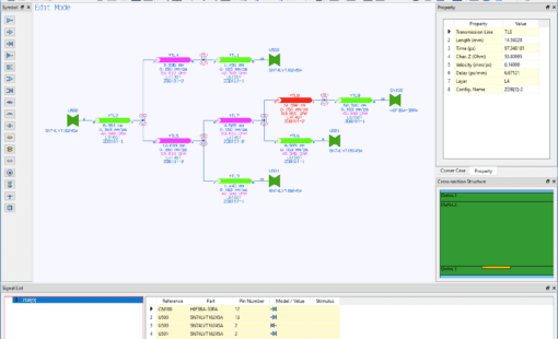
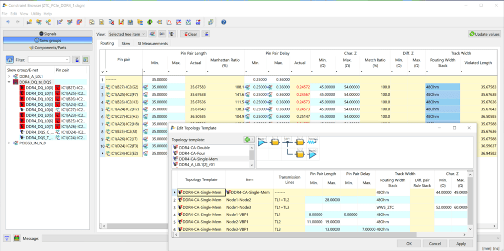
In the essential pre-layout phase, you are recommended to define the relevant high-speed constraints and to optimize the topology of critical nets (e.g.; double data rate signals). This early planning sets the stage for a robust physical design, reducing costly errors downstream and ensuring your project stays on track.
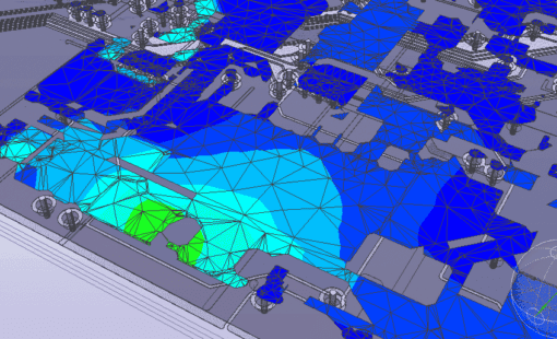
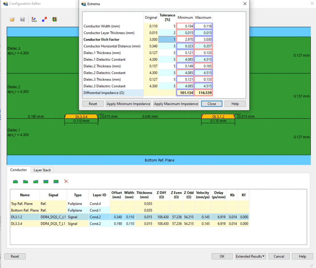
Our integrated EM field solver supports lossy interconnect models, manufacturing Tolerances, and material roughness, which empowers you to plan impedance meticulously. This approach minimizes signal loss and maximizes performance, ensuring your designs meet high standards.
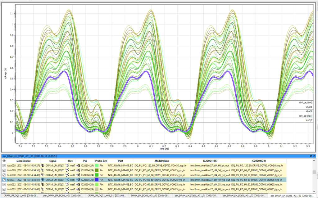
Experience rapid, interactive time-domain simulation that provides precise timing, reflection, and crosstalk analysis. Swiftly identify and rectify potential signal integrity issues, saving time and resources.
Efficiently manage your simulation library with a wide range of supported models, ensuring access to the necessary resources for accurate and reliable signal integrity analysis.
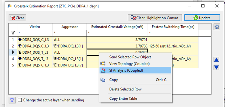
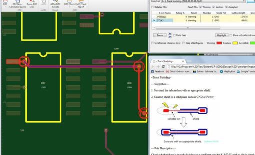
CR-8000 allows a fast crosstalk screening based on field solver results and assigned device models ( Crosstalk Estimation report), while a further detailed crosstalk simulation can be performed to proactively mitigate interference issues and preserve signal integrity.
Utilize SPICE and S-parameter-based models in the time domain, offering versatile modeling options for your signal integrity analysis, allowing you to tailor your approach to the specific needs of your project.
By utilizing IBIS buffer models, your analysis becomes highly compatible with industry standards, ensuring seamless integration into your workflow and adherence to established norms. The support of Power-Aware IBIS models allows to include effects like SSN (Simultaneous Switching Noise) in your analysis.
Fine-tune your design with parameter sweeps, allowing you to optimize your topology to meet specific requirements and ensure peak performance in various scenarios.
The usage of S-Parameter data in time domain simulation requires the transfer from time domain into frequency domain. This vector-fitting process is supported by AI/ML technology to identify best fitting parameters for the structure of interest.
Delve into the automatic timing, skew, and signal integrity measurement results to gain in-depth insights into your design’s performance.
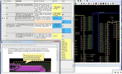
Gain a comprehensive understanding of how manufacturing tolerances and material properties impact signal integrity behavior. This knowledge empowers you to make qualified design decisions for greater reliability.
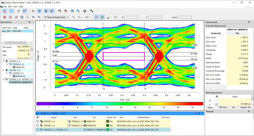
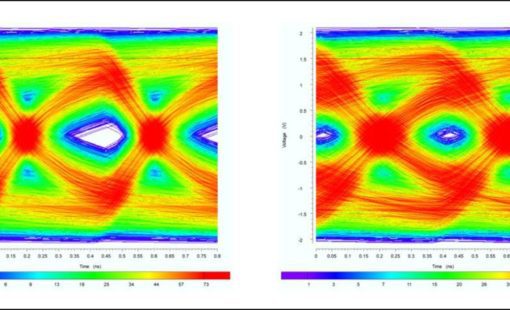
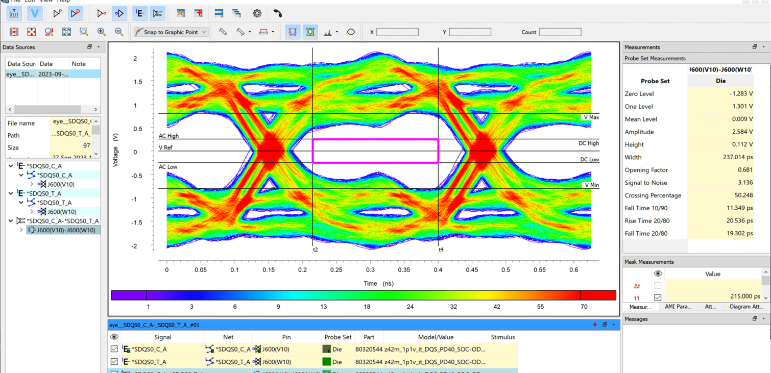
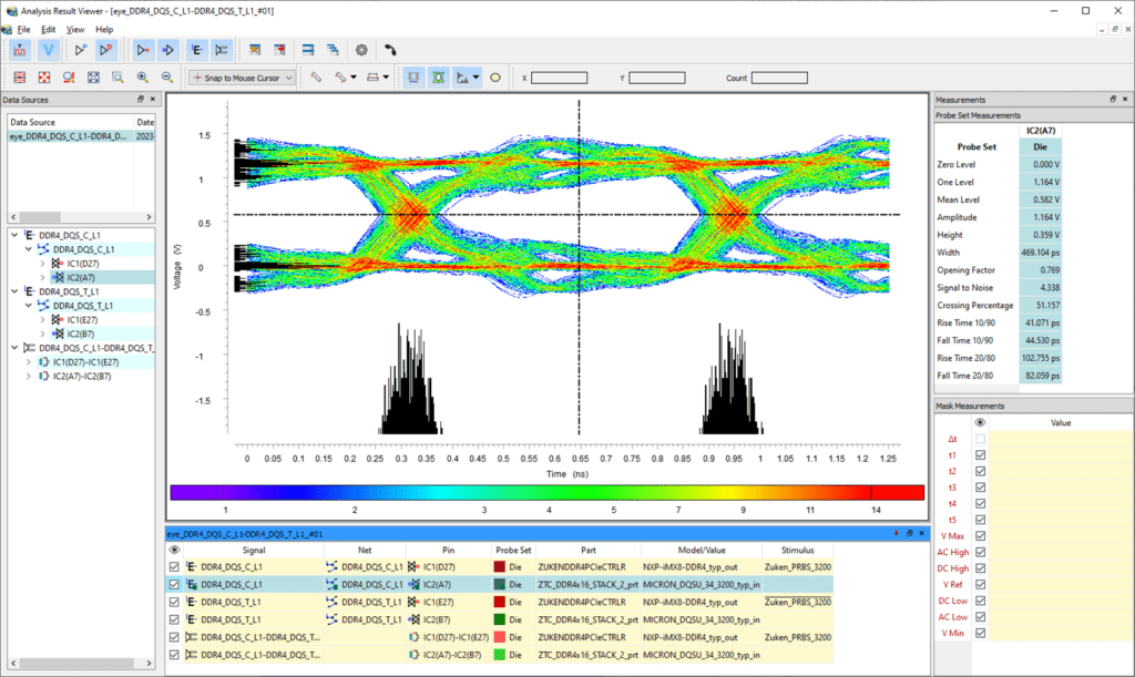
Visualize signal quality with time-domain eye pattern analysis, offering a detailed picture of your design’s performance for both parallel busses and serial links.
Precisely inspect setup and hold timing to ensure that your data transmission is reliable and meets stringent timing requirements.
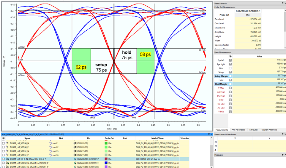
Set up eye masks to define signal quality standards and measure your signals against them. This process serves as a rigorous quality assurance step, ensuring your design meets predefined criteria.
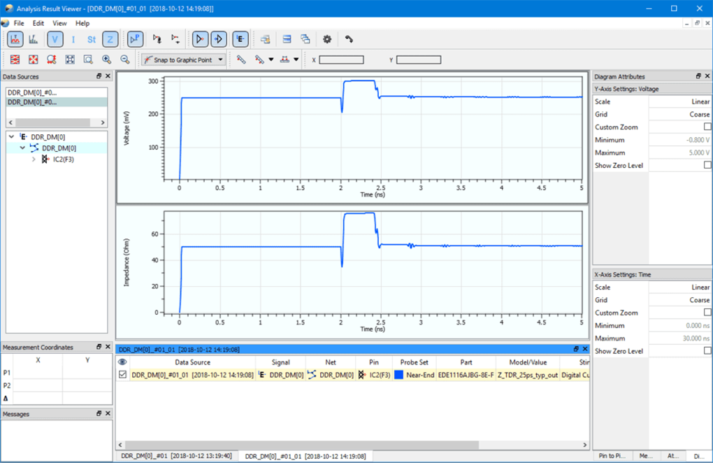
Utilize Time Domain Reflectometry (TDR) analysis to optimize your interconnects, ensuring the reliability of signal transmission and reducing the risk of signal loss.
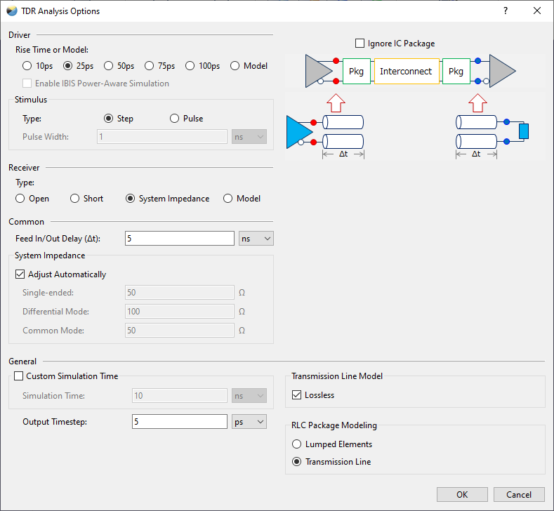
Thoroughly examine TDR impedances for both single-line and differential pair interconnects, identifying and addressing impedance mismatches to ensure signal integrity without the necessity of assigning IBIS buffer models to the devices (model-less signal integrity simulation).
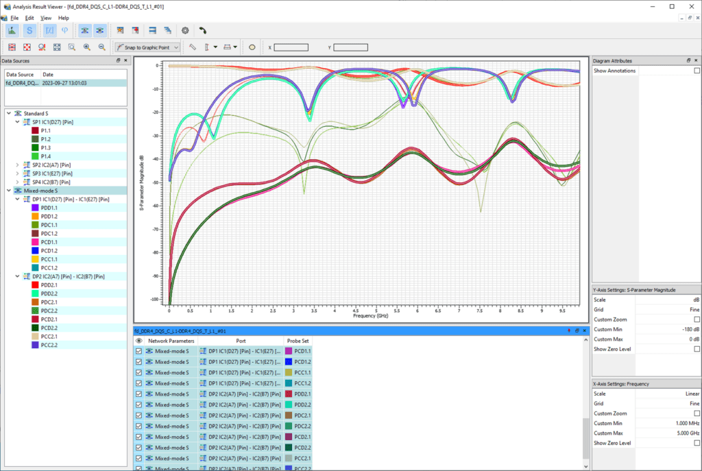
Calculate wideband S-parameters for interconnect optimization, supporting frequencies up to 15 GHz. This capability ensures high-frequency performance and reliability.
Analyze mixed-mode S-parameters to gain a comprehensive understanding of signal behavior in complex scenarios, enhancing your ability to address potential issues.
Enforce causality in your S-parameter analysis where required, ensuring the accuracy and reliability of your simulation results.
Export S-parameters to Touchstone files for seamless integration with other simulation tools, streamlining your workflow and collaboration efforts.
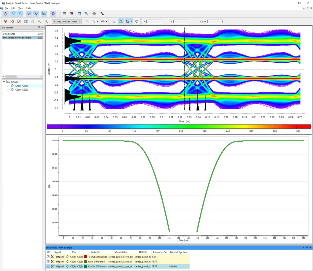
Optimize gigabit SERDES channels with AMI simulation, ensuring the reliability of high-speed data transmission and reducing the risk of errors.
Calculate the Bit Error Ratio (BER) to ensure error-free communication in your high-speed channels, providing the ultimate assurance of performance reliability.
Characterize serial links comprehensively, including S-parameter analysis, transfer function analysis, and impulse response analysis, providing a holistic view of your channel’s performance.
Account for various types of jitter (deterministic jitter, random jitter) in both the transmit (TX) and receive (RX) paths, ensuring your design can tolerate jitter and maintain signal integrity.
Visualize eye patterns and bathtub curves to assess signal quality and reliability with clarity and precision.
Simplify the parameterization of AMI models, streamlining your simulation setup and enhancing user-friendliness.
Measure eye openings and signal-to-noise ratio (SNR) to quantify signal quality and assess the margin for error, ensuring your design meets performance standards.
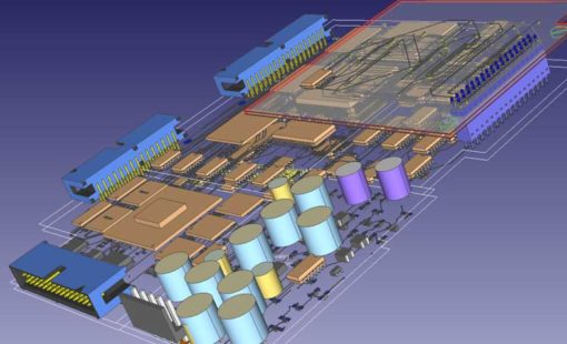
Scenario EX is a powerful simulation and analysis environment that supports checking and analysis of “what-if scenarios” from both schematic and layout data to optimize the behaviour of a circuit.
CR-8000 Design Force is the fastest, most effective PCB design solution available today. Design Force enables design teams to layout and verify their designs in the context of a complete system or product.
Related Resources
In this Webinar, you will discover how to streamline your PCB design process with CR-8000, and seamlessly integrate prototype testing results using NoiseKen for enhanced accuracy and performance.
In this Webinar, an optimized PCB design flow combining Zuken CR-8000 technology working tightly with stackup optimization capabilities provided by Polar Speedstack ™ will be presented.
Using the example of the analysis of SerDes transmission paths such as PCI Express, SATA or USB3, we explain the methodology of an analysis- and constraint-driven assembly development with CR-8000 Design Force.
In this presentation you will be introduced to the necessary steps in constraining and validation of LPDDR4 on the basis of a real design realized in CR-8000 Design Force right first time.
CR-8000 advances system-level PCB design with significant enhancements in analog simulation, SI analysis, and intelligent layout and routing
In our webinar we will provide an introduction to the challenges of signal integrity and the underlying physical effects. This will provide the basis for practical tips to address the related challenges during PCB design.
Related Blog Posts
Double Data Rate 5 (DDR5) is the next-generation standard for random-access memory (RAM). The new specification promises to bring chips that have much higher performance than the existing DDR4 modules, as well as lower power consumption. Let us show you how you can be first to market with DDR5!
To keep a good high-speed signal quality from driver to receiver on a PCB is not an easy task for designers. One of the most challenging issues is managing the propagation delay and relative time delay mismatches. Let me take you through the process...
What IC designers do to help us route high-speed PCBs
In part 1 of this blog we took a back-to-basics approach and discussed line impedance and its effects in signal integrity. As every electrical conductor comprises capacitance, an inductance, and a frequency-dependent ohmic resistance, and with increasing frequencies, these electrical characteristics will influence and distort the signal.
Impedance and impedance control are some of the oldest and most discussed topics in PCB design. They are especially important in high-speed design related to signal integrity. In this, the first of a two-part blog, we’ll go back to the basics of impedance/impedance control and consider what influences line impedance. In part two, we’ll set about controlling it.
Tips for when routing differential pairs - You can tell when something isn’t as clear as it should be. The same questions come up time and again. You ask three experts and get three different answers. Routing differential pairs can be like that. Why? Because “it depends” - on exactly what signals those pairs are carrying and what kind of PCB you’re creating.