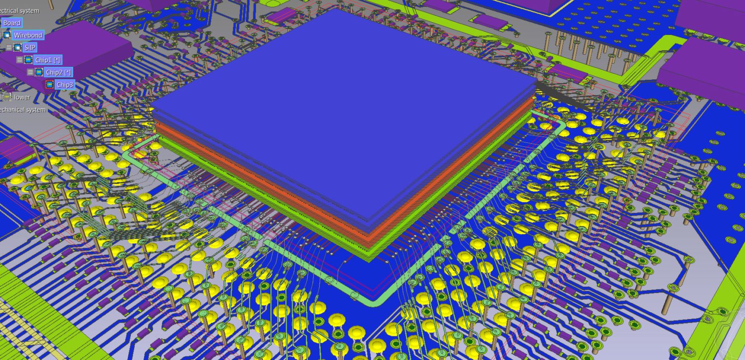
Next Generation Product-centric Design Principles
Traditional 2D PCB-centric design processes are constraining today’s highly competitive product development processes. As products become smaller, faster, lighter with more complex shapes the development process must evolve to accommodate a product-centric perspective.
Introduction
The electronic product design process is being challenged like never before, with the need to develop feature-rich, light, compact products at a lower cost in less time. To address these challenges, designers are combining chips and boards in new configurations such as complex 3D stacked structures, or new packaging technologies such as Package-on-Package (PoP) and System in Package (SiP). They are also embedding passive and active components on inner layers, inside cavities and within the dielectric of the board stack-up.
Topics:
- Multi-board design challenges
- 3D design challenges
- 3D design tools address multi-board design
- Chip-package-board co-design
- Simulation
Also see:
