Taking Electronics into the 3rd dimension
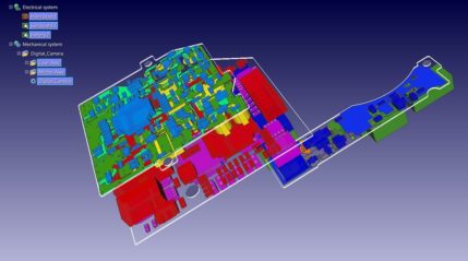
Since the introduction of CAD systems for electronic design, layout of a PCB in 2D has been sufficient for most mainstream technologies. With design pressures such as reducing cost, miniaturization, and adding more features, the use of the latest available technology has become imperative.
Discover our solutions

- Solutions

- Solutions
- Solutions
- Solutions

- Solutions

- Solutions
Electronic Engineering Blog Posts

- Blog
Zuken is taking its Simulation and Analysis Performance to the next level by introducing a new processing technology to its PI/EMI analysis tool. Multi-threading will speed up PI analysis which will give PCB designers a boost in productivity, especially when evaluating different design alternatives for PDN structures.

- Blog
Our signal integrity expert Ralf Brüning shares stories from his recent travels to various events of the PCB design industry.

- Blog
EREMS, a French enterprise specializing in the design and realization of high-tech electronic equipment and of associated software for Space, Defense, and Aeronautics uses CR-8000 and DS-CR from Zuken for the design and lifecycle management of flight electronics, ground electronic equipment, and test benches.
- Blog
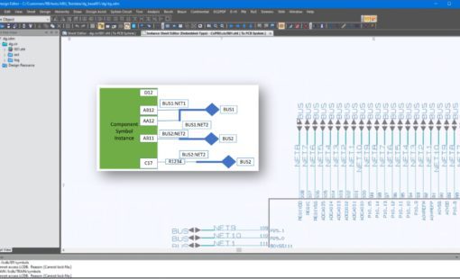
Zuken's Custom Development Group has developed a solution that enables simultaneous IC, connector, and PCB development by automating the updating of pin assignments in PCB design.
- Blog
PDN impedance is becoming more and more of a headache for PCB designers as IC vendors are defining increasingly tight so-called ‘target impedance limits’. This article explains what PDN impedance means for PCB designers and what to pay particular attention to.

- Blog
The BMWI is funding a multi-million Euro research consortium in the area of artificial intelligence research where Zuken is collaborating as one of the industry software partners.
