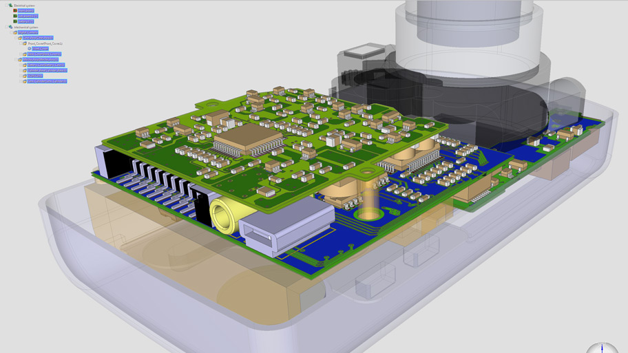
Taking PCB CAD into the third dimension
For many years, the layout of a PCB in 2D has been sufficient for most mainstream technologies. Today’s requirements, including embedding passive and active components on inner layers and through-silicon-via (TSV) technologies, call for comprehensive 3D board design and visualization capabilities.
The need for 3D
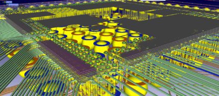
Today’s requirements include embedding passive and active components on inner layers, inside a cavity, and within the dielectric of a board stack-up. The introduction of through-silicon-via (TSV) technology has further increased the complexity of designing a product using advanced packaging technologies. 2D CAD systems cannot manage these requirements intelligently and take into consideration the necessary manufacturing rules. A true 3D PCB design system allows users to design in 2D or 3D as needed to accurately design with the latest technology and respond to market demands in high-pressure business cycles.
Adressing the multiboard design challenge
With CR-8000, Zuken provides a solution that supports optimization of a design at both the product and PCB design level.
-
3D Multi-board PCB Design
-
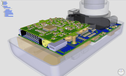
Manage all of the boards in a system, and bring them together in one view. You can select between a combination of PCBs, packages, and SoCs into one design and complete the layout of the design as a complete system.
-
Chip, Package and Board Co-Design
-
Product-centric detailed design includes 2D/3D multi-board design and implementation, FPGA I/O optimization, chip/package/board co-design, and 3D MCAD integration all in one design process.
-
3D ECAD/MCAD Collaboration
-
Import and export true 3D STEP models for components and enclosures and check for required clearance or collision to eliminate costly downstream ECAD / MCAD integration problems.
Related Products
- Products
CR-8000 Design Force is the fastest, most effective PCB design solution available today. Design Force enables design teams to layout and verify their designs in the context of a complete system or product.
- Products
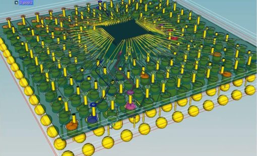
Design Force offers an intuitive, integrated environment for designing single and multi-die packages for wire-bond, flip-chip, and high density advanced IC packaging.
- Products
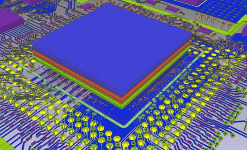
In addition to advanced PCB layout capabilities, Design Force provides chip, package, and board co-design capabilities to enable real-time 3D hierarchical design. This allows design teams to concurrently create any combination of advanced die stacks, packages, and PCBs.

- Products
Our satisfied customers
More on 3D Multi-board PCB design solutions
Check our latest webinars, white papers, blog posts and more

- Webinar
In this Webinar, you will discover how to streamline your PCB design process with CR-8000, and seamlessly integrate prototype testing results using NoiseKen for enhanced accuracy and performance.

- Webinar
With its support of 3D, CR-8000 Design Force offers the possibility of validating PCB designs against the mechanical envelope. In this session you will learn how to use formats such as IDX and JT in Design Force or, alternatively, how to import native 3D data from various MCAD systems.

- Blog
CR-8000 Design Force 2021 offers a wealth of new features and improved functionality. Check out the top benefits for PCB Designers in the newest release.
- Webinar
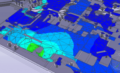
In our webinar we will provide an introduction to the challenges of signal integrity and the underlying physical effects. This will provide the basis for practical tips to address the related challenges during PCB design.
- Press Release
Key development themes for CR-8000 2020 are superior design efficiency, comprehensive system-level design and verification, and support for the latest advancements in packaging technology.
- Blog
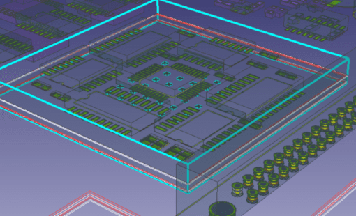
The benefits of developing all boards of a system concurrently on a single CAD canvas. Stacking PCBs, as opposed to connecting with cables, in multi-board design is a current and highly popular trend, as manufacturing costs are reduced and reliability improved.

