Multi-board constraint browser to view and analyze system level interconnects.
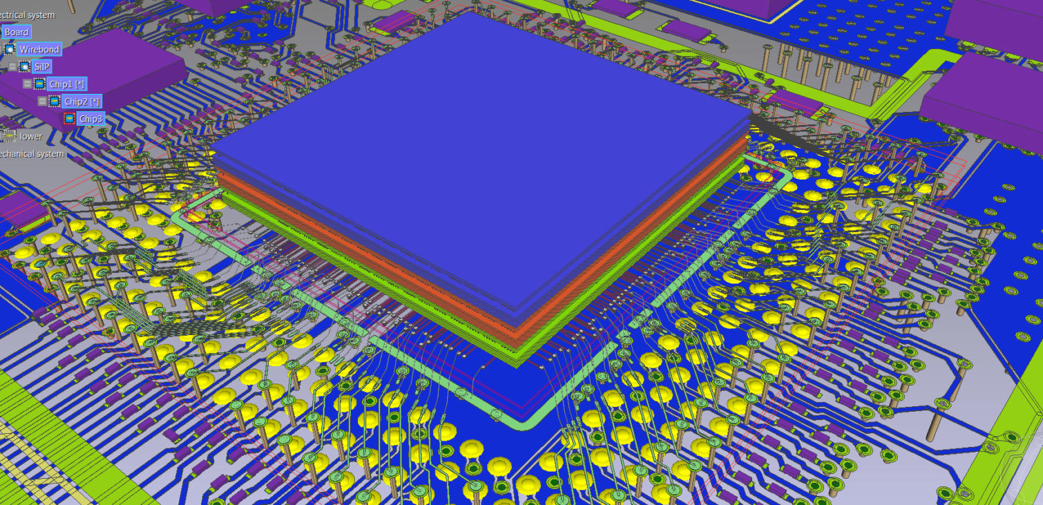
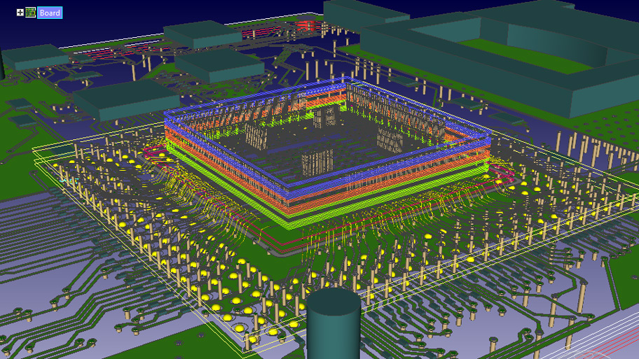
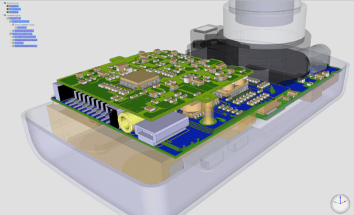
In addition to advanced PCB layout capabilities, Design Force provides chip, package and board co-design capabilities to enable real time 3D hierarchical design. This allows design teams to concurrently create any combination of advanced die stacks, packages and PCBs.
Multi-board constraint browser to view and analyze system level interconnects.

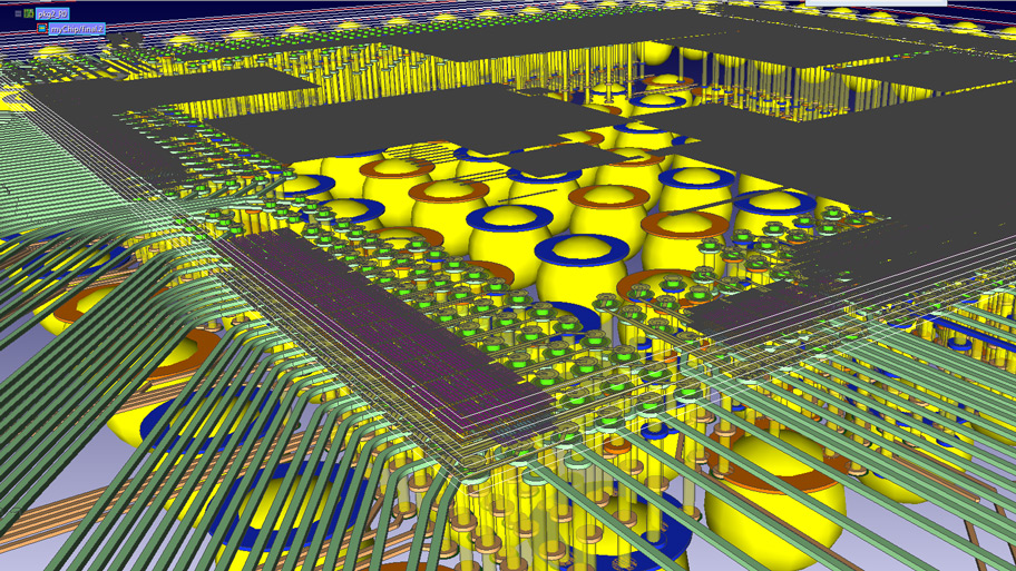
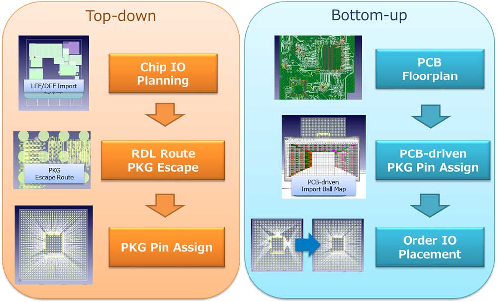
Automatic ball assignment with the ability to optimize complex routing solutions

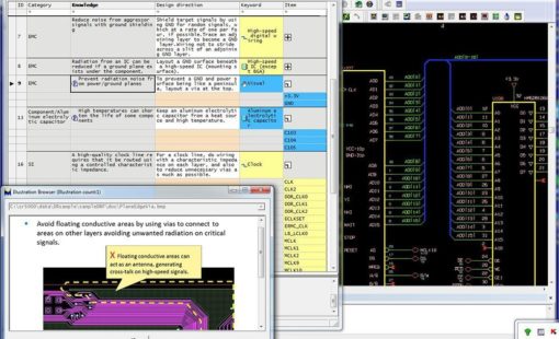
Single environment for high-speed design with constraint management and SI and PI analysis

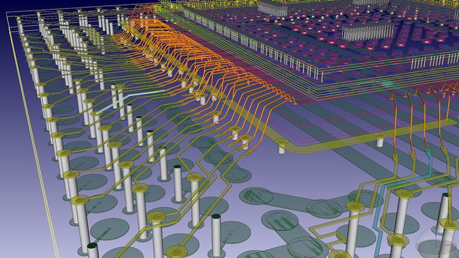
Powerful routing engines for rapid feasibility studies or detailed RDL and bump escape routing of signals and power and ground nets
Comprehensive system co-design recognizes the interaction between chip, package, and board data to reduce complexity, size and cost of the overall system.
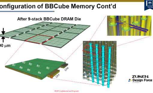
Design Force chip, package and board co-design provides a technology-rich and device-rich design environment for implementing traditional and advanced node design structures like die + package + PCB, SiP, PiP, and interposer + TSV.
Design Force Chip-Package-Board Co-Design provides a single environment solution for maximum system optimization.
Design Force supports integrations to best-in-class tools from partners such as ANSYS, AWR, Agilent and Synopsys for RF, Full Wave FD/TD, power integrity, and thermal extraction and analysis. This allows designers to address key issues early in the design process.
Produits optionnels
Les options suivantes peuvent être ajoutées pour étendre la fonctionnalité de Design Force
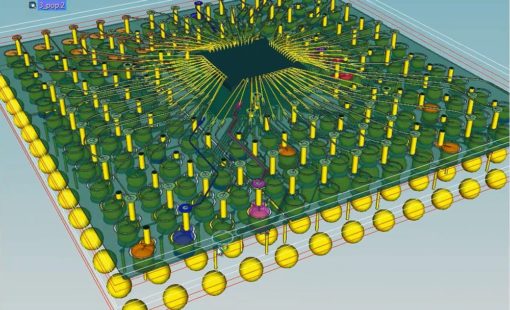
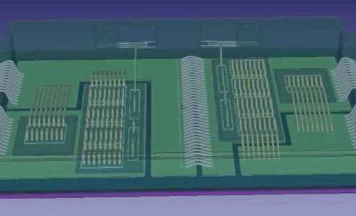
Design Force offers an intuitive, integrated environment for designing single and multi-die packages for wire-bond, flip-chip, and high density advanced packaging.
Graphical Pin Manager offers an effective FPGA / PCB co-design environment providing support for the latest devices offered by FPGA vendors
CR-8000 Design Force is the fastest, most effective PCB design solution available today. Design Force enables design teams to layout and verify their designs in the context of a complete system or product.
Pour en savoir davantage via nos webinaires, blogs, communiqués de presse et plus encore...
Post layout extraction of single and coupled (crosstalk) routed traces; What-if analysis; Cross-section view for traces.
A simulation environment for post layout signal integrity simulation.
A powerful PCB-FPGA co-design environment that enables exchange of I/O and constraint information between PCB designs and FPGA designs.
A simulation environment for Power Integrity (AC impedance and de-coupling impact, DC voltage drop, current analysis) and electro-magnetic interference (EMI full board screening, differential mode, common mode, power bus noise).
Fast and easy check of the current density of a layout structure towards a given maximum.
Related Resources
Find out more via our webinars, blogs, press releases and more...
Zuken a signé un accord de développement conjoint avec IBM pour innover dans l'intégration 3D des circuits, accélérer le hardware pour AI et optimiser les workflows EDA. Cette collaboration se concentre sur l'intégration hétérogène de puces, l'évaluation des accélérateurs d'apprentissage profond, let les tests de fiabilité. Ce partenariat souligne l'engagement de Zuken à stimuler l'innovation dans la conception de puces alimentées par l'IA et les solutions de packaging de semi-conducteurs de prochaine génération.
Zuken helps to overcome design challenges associated with 3D integration in the pursuit of next-generation semiconductor technologies.
The typical design flow for a power module is in MCAD, where only structural analysis is possible. Moving to a new design flow using CR-8000 Design Force also allows for electrical analysis too. This webinar will demonstrate the features and benefits of this new design flow.
Chip-Package-Board Co-Design with CR-8000 Design Force