On-demand webinar
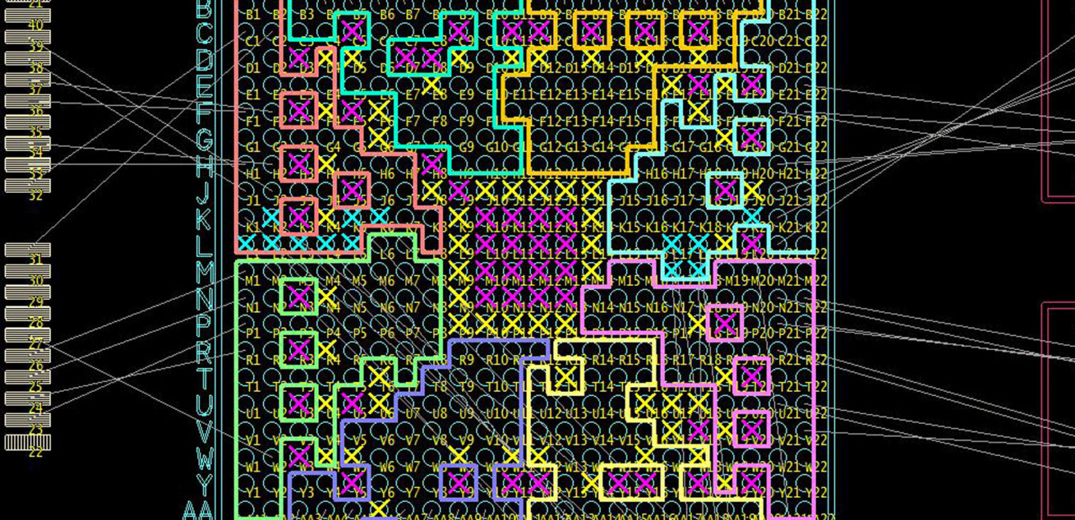
Making FPGA pin assignments without the consideration of component placement and routing can not only impact timing but make the PCB unroutable. This webinar will demonstrate an effective FPGA/PCB co-design environment utilizing the latest devices offered by FPGA vendors, such as Xilinx, Altera, Lattice, and Microsemi. Design teams will be able to easily communicate I/O and constraint information on FPGAs or other high-pin-count devices anytime during the design process.
The webinar will explore various points in the design flow where co-design of the FPGA or other programmable devices and board layout can take place; this includes library part creation, schematic entry, I/O optimization and pin assignment management during board layout. Improve your design process and the development of programmable devices in parallel to the PCB design eliminating unnecessary design iterations.
What you will learn:
- How to optimize your FPGA pin assignment for PCB design
- How to share FPGA design data with layout engineers in an automated, error free approach
- How to share connectivity and pin assignments required by PCB layout with FPGA designers
- How data synchronization between the FPGA, PCB and schematic design data can avoid unnecessary design iterations and eliminate manual information exchange
Who should attend:
- Engineering managers, hardware engineers, FPGA engineers, PCB designers
Duration:
- 36 minutes
