
PCB Design Excellence Award
Zuken Supports PCB Design Excellence in Germany with FED PCB Design Awards
27 April 2016 – Munich, Germany – Zuken has announced its sponsorship of the 2016 FED (Association for Electronic Design) PCB Design Awards, which recognize smart and sophisticated PCB design. Previous winners of this biennial award have benefited from industry recognition and new business opportunities.

Ralf Bruening, Senior Consultant at Zuken, said: “We believe that good PCB design education is important to the future competitiveness of German industry. As the only global vendor to offer both PCB and electrical design solutions, Zuken has first-hand experience of the value of good PCB design when working on today’s increasingly complex mechatronic products.”
Erika Reel, FED Executive Director, said: “The PCB Design Award honors the work of designers whose effort is often lost in the process of hardware development. The designers have to make the technically impossible possible.”
Prizes will be awarded across four categories: 3D Design; High Power; High Wiring Density/High Transfer Rates (HDI); and Special Creativity. Deadline for submissions is 31 May 2016 and application forms can be downloaded here. Entry is open to all PCB designers in Germany, Austria and Switzerland.
Award winners will be announced at the 24th Annual FED Conference on 15-16 September 2016 in Bonn.
FED is the professional association for design, PCB and component manufacturing in German-speaking countries. The association is committed to helping engineers in German-speaking countries become certified interconnect designers, helping those who typically train across a broad variety of disciplines to develop the specialized skills needed for companies to compete globally.
– ends –

- Press Release
octobre 21, 2026
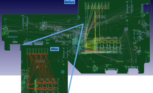
CR-8000 2026 Streamlines PCB Development With New Automation and Reuse Capabilities
CR-8000 2026 introduces new PCB design automation, placement analysis, routing, and design reuse capabilities focused on reducing repetitive work across schematic development and PCB layout. New functionality includes automated schematic routing, Main Path View, AI-assisted Smart Design Reuse, and expanded AIPR routing controls.
Read now
- Products
octobre 20, 2026
What's New in CR-8000 Release 2026
Zuken announced CR-8000 2026, a new release of its PCB design platform that adds automation, placement analysis, and design reuse capabilities to support engineering productivity across schematic development and PCB layout.
Read now
- Press Release
mai 28, 2026
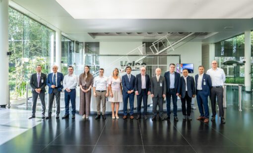
Valeo et Zuken unissent leurs forces pour redéfinir la conception électronique automobile
Valeo et Zuken collaborent à travers le Zuken Valeo InnoLab afin de créer une plateforme ouverte de conception électronique assistée par l’IA pour l’ingénierie automobile. Cette collaboration associe l’architecture IA de Zuken aux agents IA et à l’expertise industrielle de Valeo afin de réduire les délais de conception, renforcer la continuité numérique et soutenir une conception électronique robuste sur l’ensemble du processus de développement.
Read now
- Press Release
septembre 04, 2025
Participating in "JOINT3" Consortium to Develop Next-Generation Semiconductor Packaging
Zuken Inc. has joined the JOINT3 consortium—an industry co-creation platform led by Resonac to accelerate the development of next-generation semiconductor packaging materials, equipment, and design tools for panel-level organic interposers—where Zuken will contribute its CR-8000 Design Force expertise to help demonstrate, optimize, and evolve design and manufacturing processes that address the growing demand for 2.xD and 3D semiconductor packages in applications such as generative AI and autonomous driving.
Read now