Zuken joins the UCLA CHIPS consortium
May 22, 2019 – Westford, MA, USA – Zuken has joined the UCLA Center for Heterogeneous Integration and Performance Scaling (CHIPS), a collaborative academic / industry research endeavor, to develop solutions to address the challenges associated with the growing demand for computing power in heterogeneous computing environments.
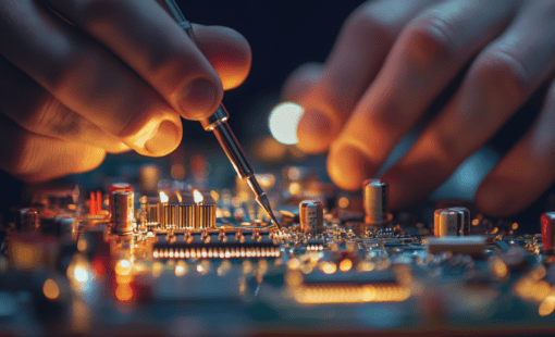
The UCLA CHIPS consortium consists of industrial partners from material suppliers, equipment manufacturers, foundries to system integrators, and includes support from universities and government agencies and industrial consortia, working collaboratively to develop new packaging technologies and system architectures and develop the next generation workforce. Zuken’s role in the consortium is to enable the team at UCLA CHIPS to utilize the system-level design capabilities of CR-8000 to layout and optimize interconnect structures between bare dies on the substrate level, along with using CR-8000 Design Force as part of the engineering curriculum to educate students in learning how to design and solve high-speed issues.
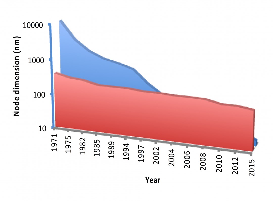
“Classical CMOS scaling has achieved an 3000X reduction in feature size over the last several decades”, explains Prof. Subramanian S. Iyer, Distinguished Professor at the UCLA Electrical and Computer Engineering and director of UCLA CHIPS. “Although it is still continuing, development and manufacturing costs are rising dramatically. At the same time, other aspects of the system such as the package and board miniaturization have not kept up, while the required effort for integrating more and increasingly diverse functions in a SOC approach is growing exponentially.” UCLA CHIPS is therefore looking beyond SOC integration at the system level: “At CHIPS we are focused on packaging and system level integration schemes to improve the overall system performance rather than improving the individual packaged components”, says Prof. Iyer.
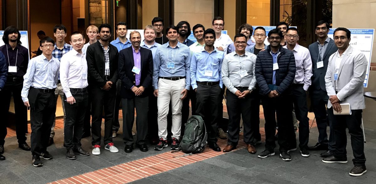
slide 1 of 3
Introducing a Moore’s Law for Packaging
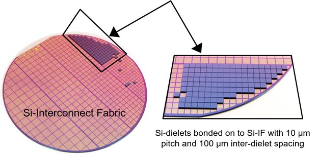
UCLA CHIPS has pioneered the concept of small dielet integration directly on a Silicon-based interconnect fabric (Si IF) or a flexible Fan-out wafer-level Package (FlexTrate*). This allows for extremely tight integration of heterogeneous dies leading to a heterogeneous System on Wafer. Allowing us to scale the package significantly – a veritable Moore’s Law for packaging. Inter-die connections may be scaled from BGA pitches of several hundred microns to a few microns and inter-die spacing may be reduced down to 20 m. This allows for significant improvements in latency, bandwidth and energy per bit over conventional packages.
Through its ability to model and layout complex designs on a system level in 2D and 3D, Zuken’s CR-8000 electronic design environment is ideally suited to model the complex die stack-ups and interposer designs required by the Silicon Interconnect Fabric and FlexTrate paradigms. As part of its corporate commitment to engage with customers in the investigation of new solution approaches, Zuken is providing design tools and services both for the CHIPS initiative and for electrical engineering course work in the UCLA curriculum.
Targeted solutions for today’s complex product development requirements
Humair Mandavia, Chief Strategy Officer and head of Zuken’s SOZO Center in San Jose, CA, comments: “Our R&D team in San Jose has been established to collaborate more closely with our customers and partners in Silicon Valley and across the US to help identify new technologies and methodologies for hardware design. Our partnership with UCLA CHIPS is another example of this approach that is fruitful for both Zuken and our customers: It puts us into an ideal position to provide more timely and targeted solutions for today’s increasingly complex product development requirements.”
For more information, visit https://chips.ucla.edu/
– ends –
*About FlexTrate
FlexTrateTM uses biocompatible polydimethylsiloxane (PDMS) as the packaging mold compound in the Fan-Out Wafer Level Packaging (FOWLP), which offers significant advantage in reducing die shift, and wafer warpage compared to conventional epoxy-based molding compounds (EMC) due to its’ lower glass transition temperature and Young’s modulus values. The CHIPS FlexTrateTM platform is also a key enabler of heterogonous integration on flexible substrates, where heterogeneous dies are integrated close to each other on a flexible substrate and interconnected using wafer level processes.
Source: https://chips.ucla.edu/research/project/5
Press release text and images are available for download here
- Press Release
mars 24, 2025
Zuken rejoint le IBM Research AI Hardware Center pour développer des solutions matérielles de prochaine génération pour l'intelligence artificielle. Zuken a signé un accord de développement conjoint avec IBM pour innover dans l'intégration 3D des circuits, accélérer le hardware pour AI et optimiser les workflows EDA. Cette collaboration se concentre sur l'intégration hétérogène de puces, l'évaluation des accélérateurs d'apprentissage profond, let les tests de fiabilité. Ce partenariat souligne l'engagement de Zuken à stimuler l'innovation dans la conception de puces alimentées par l'IA et les solutions de packaging de semi-conducteurs de prochaine génération.
Read now

- Webinar
mars 21, 2025
AI-Based PCB Place and Route CR-8000 Webinar: Zuken recently announced the upcoming release of the industry’s first AI-based PCB place and route product - Autonomous Intelligent Place and Route (AIPR) - This webinar will examine how companies and users will benefit.
Watch Now

- Webinar
octobre 16, 2024
Advanced Electronics Collaboration: Zuken DS-CR and Dassault Systèmes’ 3DEXPERIENCE Platform Discover how Zuken’s CR-8000/DS-CR integrates with Dassault Systèmes’ 3DEXPERIENCE Platform, providing robust solutions for efficient data management and collaborative workflows between electrical and mechanical design teams.
Watch Now
- Webinar
septembre 17, 2024
Optimizing PCB Design: From Schematic to Prototype Testing with CR-8000 and NoiseKen In this Webinar, you will discover how to streamline your PCB design process with CR-8000, and seamlessly integrate prototype testing results using NoiseKen for enhanced accuracy and performance.
Watch Now