Key Theme: Design Efficiency
Major enhancements in the areas of schematic design, FPGA optimization, skew group routing and support of back drilled vias. Streamlined routine design work through extended semi-automatic routing functionality.
Zuken reveals details of release 2020 of its advanced 3D multi-board PCB design environment CR-8000. Key development themes for CR-8000 2020 are
Many enhancements contained in the new release were developed in close collaboration with Zuken’s global customers in business sectors, including electronics, high tech, automation, automotive, aerospace, and defense. As product complexity increases, these businesses are searching for opportunities to increase design performance and process resilience.
Major enhancements in the areas of schematic design, FPGA optimization, skew group routing and support of back drilled vias. Streamlined routine design work through extended semi-automatic routing functionality.
Design Gateway, the schematic capture and engineering environment of CR-8000, has been significantly enhanced by the move to a native 64-bit environment for improved rendering and performance, and the introduction of a new (Windows 10 style) graphical user interface that has been designed to provide enhanced usability and performance.

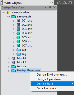
A redesigned Design Tree View improves navigation in large designs. In addition to the hierarchical representation of folders and sheets, the Design Tree View now includes a design resource folder which contains a detailed history of output files (such as netlists and BOMs) and log files documenting the full design history, as well as a listing of the specific design rules applied in the current design.
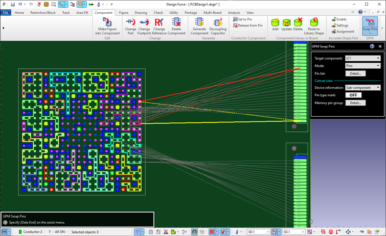
Board designers can now perform FPGA gate and pin swaps directly in Design Force, the board layout and routing application of CR-8000. All changes made in Design Force will now be automatically back-annotated to Zuken’s FPGA and board co-design environment Graphical Pin Manager.
Extended use of semi-automatic routing provides significant efficiency gains by streamlining the time-consuming task of optimizing signal lengths for skew control. Signals can be highlighted automatically in color codes to indicate their compliance with the skew constraint defined in the circuit design. Green indicates ok, red indicates too short and blue indicates too long. In this way, skew violations can be easily identified and addressed by increasing or shortening tracks lengths using Design Force’s sophisticated routing tools.

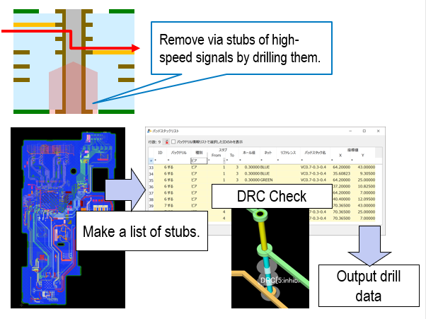
To reduce potential antenna effects of unused plated vias in high-speed boards, Design Force has been enhanced to automatically identify via stubs for back drilling during board production. Drilling data for back drilling vias can now be generated in a one-stop operation during board layout eliminating the time-consuming task of manual identification and generation of drilling outputs.
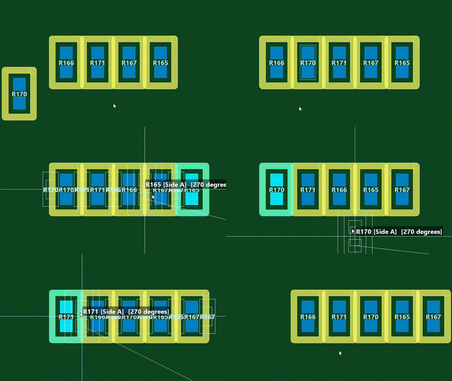
Routine design work benefits from the extended availability of semi-automatic functionality. The component placement functionality has been extended to include automated push aside algorithms that make room when components are added; for dense areas, track widths can automatically be reduced to user-defined values. Moving between active layers is now made easier by using the upward and downward key.
Optimized electro-mechanical design flow for flex-rigid PCBs and directly embedded multi-domain analysis capabilities
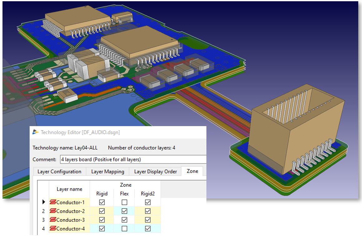
Geometries and dimensions can be directly imported from all industry standard MCAD design tools. Mechanical outlines are automatically extracted by Design Force and the PCB design data updated automatically.
Using Design Force’s 3D design capabilities, flex parts can be manipulated and checked for interference and clearance directly in the PCB design environment. Inversely, updated and verified flex PCB date can be exported back to M-CAD.
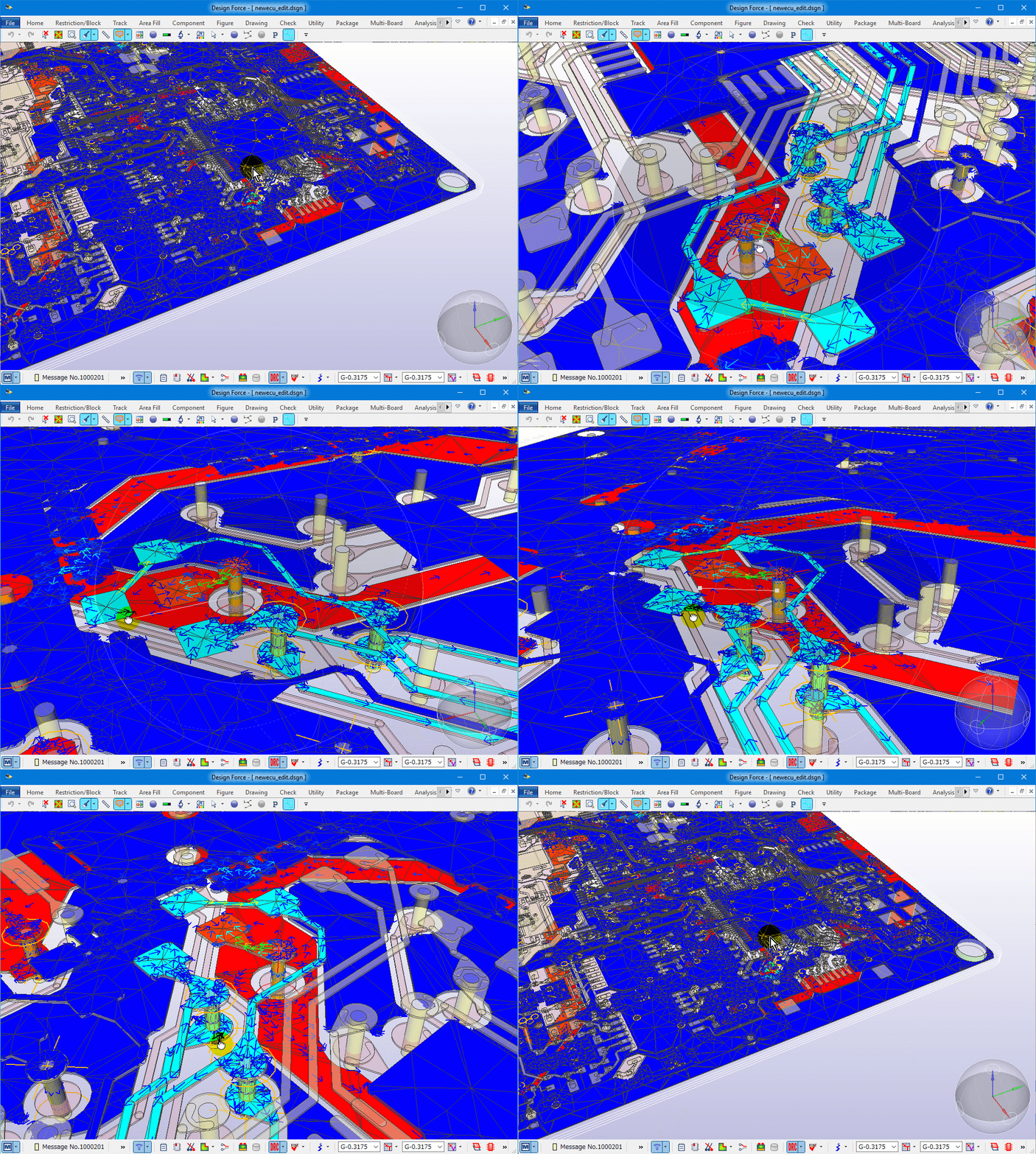
A direct integration of best-in-class analysis solutions from Zuken’s partners Keysight and ANSYS enables the analysis of PCB designs across multiple domains. Various techniques of simplifying board design details data have been introduced to reduce the time for meshing and contribute to stabilizing simulation results.
2.5D and 3D data can be transferred directly from Design Force to the Keysight RF design and analysis environment, where the layout characteristics can be extracted and optimized in a what-if-approach.
Similarly, ANSYS simulation tools for signal integrity, power integrity, and EMC as well as electromagnetic field analysis, thermal analysis, and structural analysis can now be launched directly from the CR-8000 environment.
To cover the latest advances in the area of packaging technology, CR-8000 Design Force has received additional as well as enhanced functionality in the areas of tile bump planning and 3D wire bond design for power modules
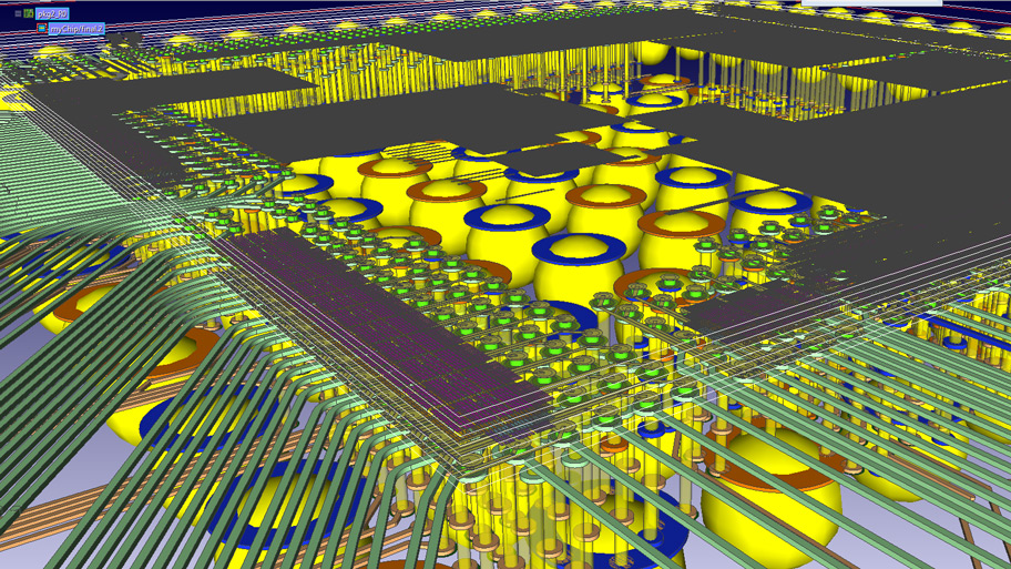
The bump design for Flip Chip Package (FCPKG) designs needs to consider both system-on-chip and package design constraints to establish an optimal solution in an iterative process. Using today’s industry-standard design tools, it is difficult and time-consuming to run many iterations, as changes need to be coordinated between the different tools with the help of spreadsheets. With hierarchical multi-domain capabilities in an end-to-end environment, Design Force supports both the design of individual packages and boards, and a concurrent implementation and optimization of chips, packages, and boards.
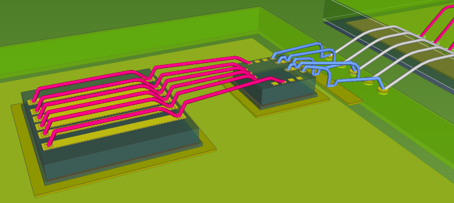
Due to the growth of the IoT and connected devices, the demand for power modules is projected to grow drastically. Power modules are placed as ceramic child boards on a base board and connected by means of 3D bonding wires. With today’s design tools, designs using power modules frequently involve disconnected tools, with the wire connections frequently being designed on M-CAD tools. By supporting 3D multi-board co-design and SiP (system-in-package) wire bond designs in one consistent environment, CR-8000 Design Force 2020 provides a consistent environment for the system-level design and verification of power modules
