New tools allow concurrent creation of advanced stack dies, packages and PCBs.
In pursuit of feature-rich, light, compact products at a lower cost in less time, designers are increasingly creating complex multi-board products and using new packaging technologies to pack integrated circuits more closely together. Multi-board designs create new challenges such as planning and management of interconnects at the system level. The greater complexity of new packaging technologies means components need to be more tightly coordinated with one another so that pin assignments can be optimized for small size and minimum layer count substrates. Traditional 2D printed circuit board design systems are not well-suited to address these challenges because they are used to design one PCB at a time in isolation from the other PCBs within a product and also in isolation from the ICs, packages and enclosure.
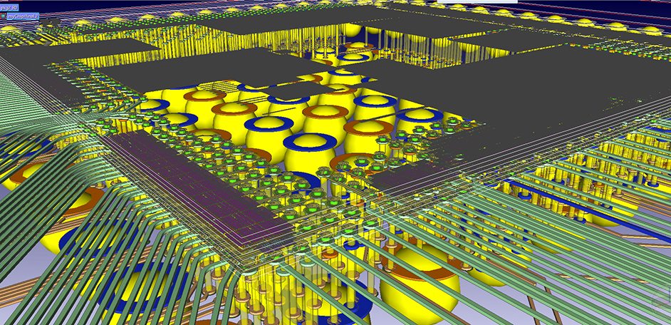
A new generation of 3D multi-board product-level design tools manages multi-board placement in both 2D and 3D and enables co-design of the chip, package and board in a single environment. Multi-board design makes it possible to create and validate a design with any combination of system-on-chips (SoC), packages and PCBs as a complete system. Chip-package-board co-design enables designers to optimize routability via pin assignment, and I/O placement to minimize layer counts between the package, chip and board. The new design methodology makes it possible to deliver more functional, higher performing and less expensive products to market in less time.
Related Products and Resources

- Products
Today’s Desktop PCB Design tools require better connectivity to the outside world. eCADSTAR offers a newer level of connectivity that brings users closer to their parts providers than ever before. This allows Engineers to selected parts and drag them directly to their design. Add the additional functionality of high power Signal integrity verification and Power integrity analysis and you have the Ultimate Desktop PCB Engineering solution.

- Products

- Products
Zuken’s engineering data management platform DS-CR has been created to support the specific demands of PCB design data management. It combines multi-site library, design data and configuration management into a unified engineering environment.

- Products
Building a competitive product today is much more difficult than a few years ago. Existing PCB-centric design processes are limited to a single PCB and do not provide the necessary tools for today’s competitive product development environment. PCB-centric design processes are falling behind.


