In the recent past, advanced packaging design simply meant wire bonding a die onto some type of substrate. This could be considered the origin point of advanced packaging tools. Now, this realm of advanced packaging encompasses much more. The packaging design challenges exist in multiple spaces, some electrical, some mechanical, and some a hybrid of both disciplines. So, let’s discuss some of these new advanced packaging design requirements and the processes to tackle them.
Chiplet-level design processes
Some of the biggest challenges in chiplet-level design are route optimization and maintaining a desirable time-to-market. By looking at chiplet issues as a system, you can optimize your entire design. One way to achieve a high level of optimization is to reach into the RDL level of the chip and optimize that interconnect through multiple fabrics right down to the PCB level. This process ensures the most electrically desirable interconnect and the most routable outcome at the various levels. When using a design tool that provides visibility into these multiple design spaces, the process of examining swaps and tradeoffs to improve the route pattern or electrical performance yields significant time-to-market benefits.
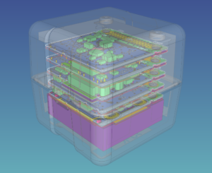
System-level design must include mechanical
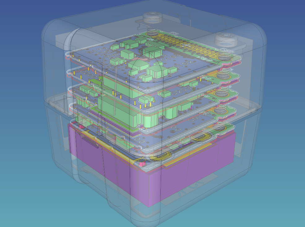
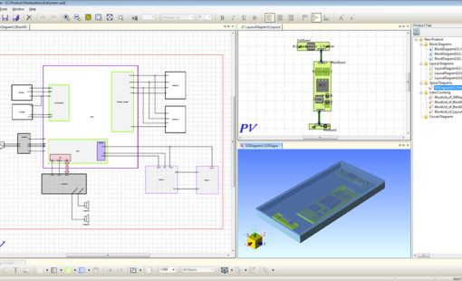
More and more, we are seeing mechanical requirements driving package and PCB design considerations. Therefore, the necessity to merge these two disciplines into a common workspace has never been more apparent. As customers continue to shrink products to smaller form factors, the effect of PCB and packaging design is extensive. Add to that equation that many products have varying functionality or purposes, and the need for an adaptive design process becomes clear. Therefore, merging the mechanical and electrical aspects into a common design space ensures good decision-making without the necessity for multiple data round trips between mechanical and electrical disciplines.
The new packaging challenge of power module design
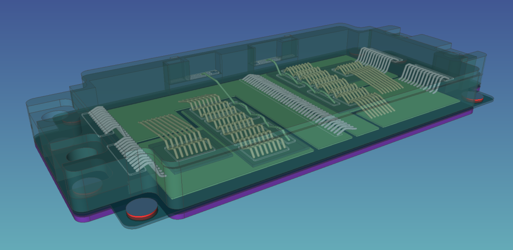
In the old era of automotive design, 12-volt systems were well known. The systems were easily accommodated in the hostile environment faced by automotive designers. Meanwhile, in the new world of EVs, those 12-volt systems are now a side note in the design process. For example, 48-volt systems and above (well above) create new challenges for PCB and packaging design processes. Consequently, these challenges place significant mechanical requirements on the electronic design form factor. They also create the necessity for in-component, component-to-mechanical-object, and board-to-board bond wire challenges, truly merging electrical and mechanical design into a hybrid product.
These new high voltage requirements necessitate significantly more wire bonds. In contrast, one or two bonds would accomplish the goal with the old way of doing things. Most often, engineering teams work on these high-voltage designs exclusively in mechanical CAD tools–until now. The process worked well from a mechanical perspective. However, it left the design without any electrical design rule checks, little to no netlist validation, and too many challenges for electrical simulation.
By merging the mechanical and electrical disciplines, we can explore an entirely new type of design process that leverages the best of both worlds. Therefore, designs now have netlist-based checking, true electrical-level design rules checks, and the ability to quickly simulate those electrical behaviors to validate the end product.
Visit us at ECTC to learn more
As you can see, advanced packaging design encompasses an ever-growing area of technologies and is adapting to meet modern challenges. Visit our virtual exhibit booth at ECTC. Our team will gladly show you how to tackle your most challenging designs using CR-8000.
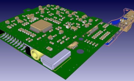
CR-8000 Design Force provides chip, package and board co-design capabilities to enable real-time 3D hierarchical design. This allows design teams to concurrently create any combination of advanced stack dies, packages, and PCBs.
ECTC is the premier international event that brings together the best in packaging, components and microelectronic systems science, technology, and education, and Zuken is proud to be participating. Stop by our virtual booth to meet the team and to learn more about Zuken’s tools for Advanced Packaging.
Related Products and Resources

- ZIW
- Products
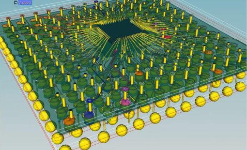
Design Force offers an intuitive, integrated environment for designing single and multi-die packages for wire-bond, flip-chip, and high density advanced packaging. Designers can start designs with early prototype input of chip and package data from the library, reuse data from IC layout tools, and take advantage of parametric wizards to streamline the creation of the system
- Products
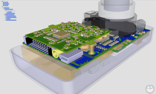
Design Force combines traditional 2D design with native 3D design and the latest human interface techniques, accelerated graphics and almost instantaneous rendering and refreshing. It is the fastest, most effective PCB design solution available today. Design Force enables design teams to layout their designs in the context of a complete system or product.
- Press Release
