According to a report by Technavio, the expectation is that the PCB market (Printed Circuit Boards) will increase by $1.9 billion by the year 2027. This level of growth should come as no surprise considering the steady evolution of technology, such as advanced communication network infrastructure to support 5G, higher demand for IoT (Internet of Things) and IIoT (Industrial Internet of Things) products, and autonomous automotive applications. As a result, engineers must find new ways to design and incorporate advances in PCB manufacturing automation to keep up with increasing product complexity.
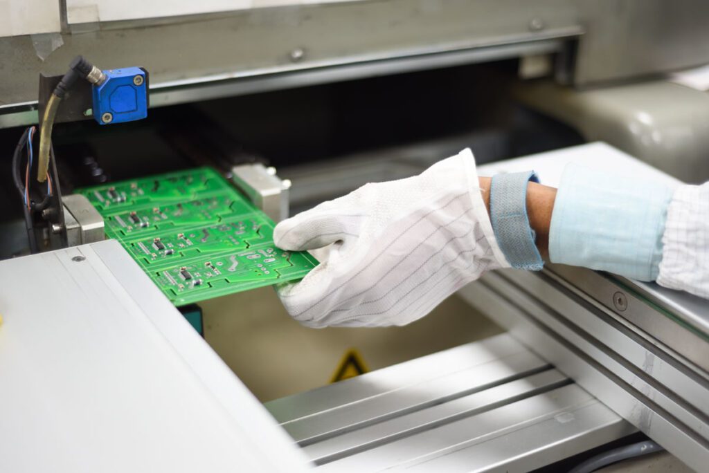
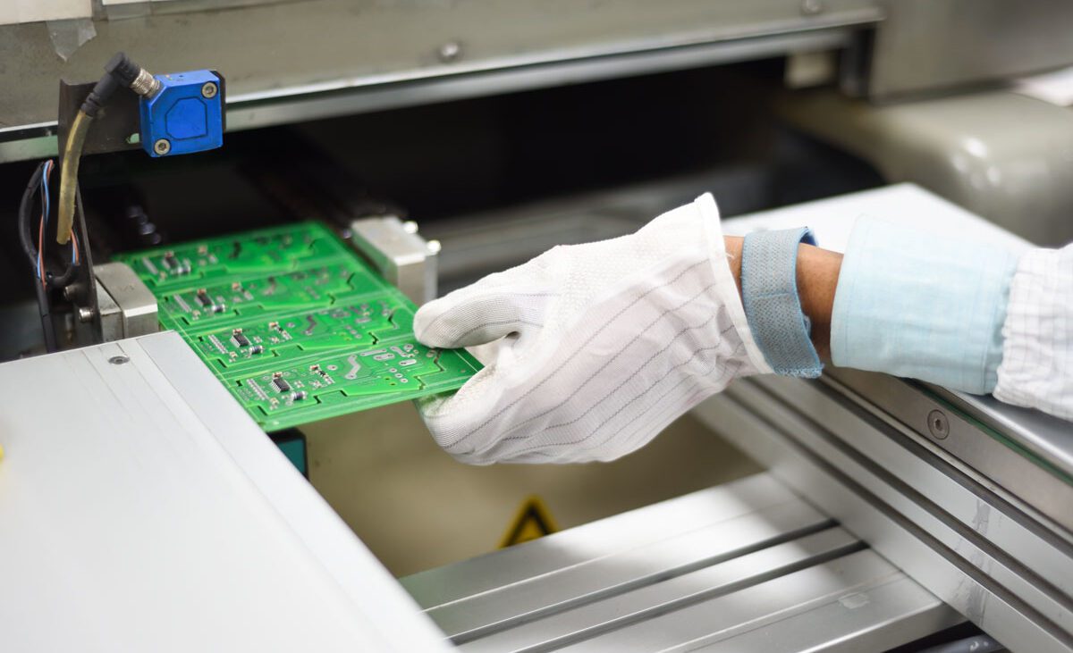
Many PCB manufacturers are turning to advanced automation. The International Society of Automation has presented several vital benefits that factory automation brings to manufacturing PCBs. These include improved production speed, better consistency, fewer PCB defects, and a more straightforward approach to miniaturization.
Advances in the Factory Automation of PCBs
In recent years, manufacturing automation of PCBs has made several advances. Areas of particular interest for manufacturers are additively manufactured PCBs, AOI and AOS, and Design for Manufacturing Tools.
Additive PCB Manufacturing
3D printing, a subset of additive manufacturing, is rapidly gaining popularity in PCB manufacturing. It is an innovative application of layer-by-layer additive manufacturing techniques instead of methods, such as etching, that remove material.
There are two ways to print PCBs, such as the one shown in Figure 2. First is printing the circuit board with hollow traces to fill later with a conductive material. The second is using a conductive material to print the circuitry directly during the additive process.
Just like 3D printing of any other object, the printer will receive a mesh file in one of the standard formats. From there, the printer will add, layer by layer, the various holes, channels, troughs, and other circuitry features using the methods described above.
3D printing for PCBs is currently limited to small production runs, rapid prototyping, and highly unique PCBs, but it fulfills a specific market need. With continued advances in 3D printing technology, it will eventually expand its usability and the size of production runs it supports.
AOI and AOS
AOI (Automated Optical Inspection) systems are inline inspection systems used in PCB manufacturing and quality control. They are a machine-based approach to discovering flaws and defects, even in complex designs like the one shown in Figure 3. These include physical defects (e.g., short circuits, open circuits, thin solder), incorrect components, missing components, surface defects (e.g., scratches, nodules), and incorrectly placed elements.
These AOI systems can specifically check PCBs for excess copper, hole breakage, spacing, and line width violations. Inspections for PCBs with components can look for excessive solder joints, insufficient solder joints, lifted leads, issues with paste registration, and solder bridging.
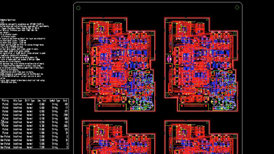
AOI systems are becoming more precise in supporting circuit boards’ high-quality, efficient manufacture. Advanced precision means fewer production line delays related to incorrect defect detection. So after detecting a defect, AI-driven AOS (Automated Optical Shaping) systems can automatically correct them.
Design for Manufacturing Tools
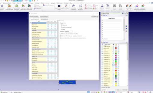
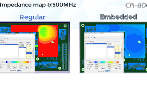
No matter how well-designed a PCB may be, there will be problems if the automation output needs correcting. Using automated systems, DFM (Design for Manufacturing) tools ensure accurate manufacturing and efficiency. Zuken’s CR-8000 DFM Center provides essential capabilities such as:
- Preparation and verification of manufacturing data by paneling up a single or combination of PCBs
- Dynamic application of fabrication and assembly checks based on any manufacturer’s specifications
- Powerful post-processing functionality to optimize manufacturability
- Support for design-anywhere-manufacture-anywhere methodology
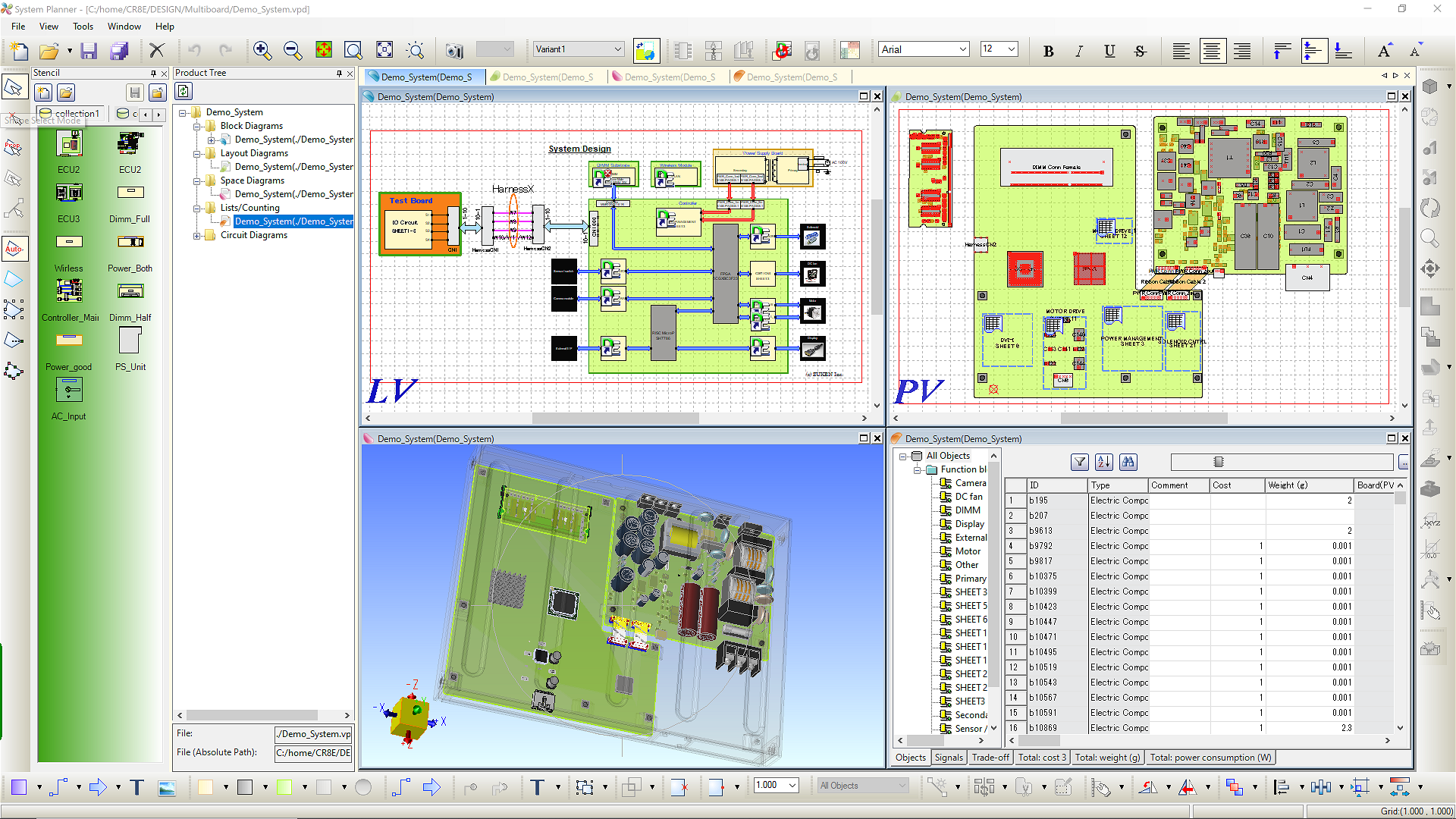
Combined with DFM Center, CR-8000 Design Force will optimize multi-board architecture, 2D/3D detailed design, and chip/package/board co-design. This tool suite is a single fabrication/assembly checking platform for any board technology (e.g., rigid, flex, LTCC, and embedded components). And the embedded rule-checking engine checks rules during design in real time. All of the above Zuken tools can then be made more capable with the addition of Advanced Design for Manufacturing (ADM). ADM allows for the creation of custom rules that can be tailored to specific processes or manufacturers. This functionality enables a more finely honed review process and the incorporation of lessons learned in previous manufacturing passes.
Zuken Design Tools for PCB Manufacturing Automation
Zuken has other PCB design tools and platforms, such as the DS-CR, for the distributed management of ECAD design data and libraries, as well as the auto-generation of PCB documentation. In addition to our enterprise tools suite, we also offer a desktop PCB design platform, eCADSTAR, which, in addition to schematic and PCB capture, offers Spice simulation, SI/PI analysis capabilities, and 3D MCAD integration.
Due to the demand for more PCBs and the increase in complex designs, PCB manufacturing automation is steadily becoming a critical requirement. With advances in additive manufacturing, automated inspection systems, and DFM tools, more engineers find it easier–and more cost-effective–to execute their designs utilizing PCB manufacturing automation.
