The advent of Artificial Intelligence (AI) is transforming nearly every sector in our modern world, with the field of Electronic Design Automation (EDA) poised to significantly benefit from this change.
As electronic devices become smaller, faster, and more efficient, the complexities of Printed Circuit Board (PCB) design continue to escalate. Consequently, by utilizing AI-driven EDA tools, the industry can pave a clear path forward to address the challenges of PCB design.
In this post, we’ll explain how AI-driven EDA can revolutionize the design process and how Zuken’s CR-8000 embraces this paradigm shift.
Automating Routine Tasks
When considering the complex aspects of PCB design, AI’s power lies within its ability to automate routine tasks, significantly reducing the manual workload of a designer.
Component placement optimization is among the most impactful areas in this domain. With traditional methods, designers manually place individual components on a PCB layout, which can take hours or even days, depending on board complexity. Still, AI algorithms can perform this task in a fraction of the time. For example, they have the ability to analyze multiple variables like electrical connectivity, thermal distribution, and signal integrity to find optimal placement for each component.
Routing optimization is another routine task that can benefit from the addition of AI technology. Traditionally, designers have had to manually draw traces between components, ensuring they meet specific design rules and constraints. To streamline this process, AI can automate routine optimization by calculating the most efficient pathways for electrical connections. This automation can even consider multi-layer routing and vias, thereby reducing the overall board size and gaining the potential to lower manufacturing costs.
Quality Assurance
AI-driven EDA tools can optimize pre-production processes by preventing mistakes and ensuring high-quality designs.
One of the most compelling applications of AI-driven EDA lies within real-time design rule checking. In conventional workflows, design rule checks are often performed at the end of the design process, making required revisions cumbersome and time-consuming. However, AI-driven EDA tools can perform these checks in real-time, flagging potential violations as they occur. This synchronous feedback allows designers to correct mistakes immediately, reducing the likelihood of errors propagating through the design.
Furthermore, AI excels in predictive analysis, particularly machine learning-based failure prediction. By analyzing historical data and learning from past design failures, AI algorithms can predict potential points of failure in new designs. AI-driven EDA can facilitate this predictive capability. It enables designers to address vulnerabilities before they become critical issues–thus saving both time and resources in debugging and redesign.
Zuken’s CR-8000: A Forerunner in AI-based PCB Design
Zuken’s CR-8000 is a leader in the EDA industry, embracing the pivotal role of AI in the future of design.
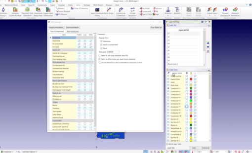
Specifically, CR-8000 Design Force–an advanced PCB design and system integration platform–utilizes AI and machine learning to automate and streamline design tasks. One of its standout features is the “Commands Using AI” function, which learns from a user’s past activities to suggest future commands to boost efficiency. Additionally, this feature captures recent operations for real-time updates and provides suggestions directly in the Graphical User Interface (GUI). Conveniently, Design Force eliminates the need for excess navigation and allows for a streamlined design process.
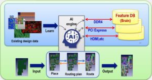
Zuken is actively investing in the integration of AI technology into its PCB design processes. Several critical areas of focus include:
- Circuit recognition and reproduction: AI will recognize circuits and components from acquired data and automatically reproduce the proven layout and routing.
- Distancing: AI will automatically adjust the distancing between components or tracks and their relative positions.
- AI-driven optimization of pin counts: AI will deliver highly accurate results, leading to shorter design times and reduced dependence on designers.
- DR optimization using AI: Based on DR check items from past data, AI will automatically extract items that must be checked in circuits and apply the appropriate check rule.
The Future of AI-Driven EDA
Between task automation and design analysis, it’s clear that AI has a significant role in modern PCB design. Zuken’s CR-8000 is harnessing the evolutionary potential of AI-driven EDA and leading the way by offering features that excel beyond task automation to substantially improve design quality.
- Blog
- Blog

- Blog
- Blog
