Scaling for Progress
The world we live in now is one where collaboration and access are standard expectations of us and our tools regardless of time and location. Even traditionally “office-only” things must scale across time and space, including ECAD tools. Successfully implementing a solution to fulfill the needs of future work models requires overcoming a variety of infrastructure challenges or rethinking how to structure projects. This is where team-based PCB design can help address some of your challenges.
Team-Based PCB Design Paradigm Challenges
The concept of team-based PCB design is not new; a few EDA vendors already offer this set of features. It gives PCB designers the platform to work on the same design concurrently, whether in the office or remotely from anywhere in the world.
Successfully implementing remote team-based PCB design traditionally required addressing the following:
- Network security access from remote IP locations.
- Network and internet latency when accessing the same design at the same time.
- Added cost – these features are often an additional cost option.
Network security – Almost every day, the headlines have incidents of data breaches and security violations. Cybersecurity is perhaps the most significant thing in IT professionals’ minds under typical circumstances, and the world has changed in such ways that security is more important than ever. VPNs are critical to maintaining security. Anyone doing remote PCB design without the safety net of a VPN is asking to be the victim of the next data breach headline.
Network latency – It is easy to confuse bandwidth with latency, and while the two are closely related, latency is particularly critical when performing real-time actions. Bandwidth measures the total amount of data throughput over time. Latency measures how long it takes to acknowledge a data packet as received. Team-based remote design is an exercise in real-time communication where low latency is critical. Selecting networks with ping values in the sub-10s should deliver a smooth concurrent design experience.
Cost – The costs associated with enterprise-level tools that support team-based PCB design can be high. Many electronics companies with smaller budgets for EDA software must rely on mainstream, commodity-based PCB design tools. Unfortunately, these tools are not intended to work in a team-based design flow. Team-based PCB design is necessary for large, complex designs requiring multiple subject matter experts to implement under time-critical conditions.

Restructuring the Process
There is an alternative that can circumvent the infrastructure challenges. If we consider a PCB design as a complex set of circuit blocks, each owned by an engineer, we can see that the design is essentially divided. We see this when a PCB designer must collaborate with two or more circuit engineers for component placement approval and high-speed routing constraint applications. The concurrency in this scenario is that two circuit designers with differing needs affect one PCB. Furthermore, circuit engineers may want to place components on their specific circuit blocks and perhaps even some routing. Sequential design is the only way to address such conditions, leaving behind the time savings of a parallel approach. How can the project change to be compatible with team-based design?
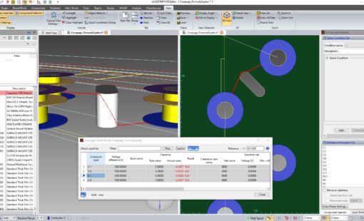
The approach Zuken offers with eCADSTAR is a bit different. It is easy to imagine how a schematic can be sub-divided into functional blocks, and there is a similar story with the PCB. The designer can parse the PCB into separate files and store it in the PCB design project folder on the remote machine. From there, circuit engineers and PCB designers can work with their specific circuit blocks. Breaking up the PCB design into separate files allows team leaders to simplify and streamline sub-section review, sign-off, and lock portions of the PCB design without having to wait for the entire board to be complete. It also allows access control of sensitive areas of the PCB. The ability to support team-based design is part of the eCADSTAR base bundle.

Team-Based Design Guidelines
Setting up team-based PCB design isn’t difficult, but there are some essential guidelines and best practices to ensure success.
- Keep it together – It is important to group complementary components in various board groups. Designs naturally tend toward this, but PCB real estate sometimes causes deviations from this paradigm. The more co-located components are, the easier it will be to logically split off and create nearly independent board blocks.
- When in doubt, split off – It may be a bit excessive to go as far as saying, “you can’t have too many files,” but erring on the side of caution can save headaches down the line. If there is a board section that kind of fits with an existing board block, but not really, it is probably a safer bet to split it off into its own section.
- Reuse for scale – Breaking off a segment of the PCB into its own block is an excellent way to create reusable, self-contained functional segments. If there is a particular reusable circuit that has a challenging layout, it can save significant time in the future to lay it out and create connection points that enable the reuse of that block in the future. This is particularly important for high-net-count or high-pin-count devices such as DDR and FPGA.
No matter what tools you’re using, see if your vendor supports true divided design capability. This will help to save time, monitor design progress, and allow you to archive designs in reusable blocks for future use. The future paradigm of PCB design will be one of the distributed resources working on concurrent designs simultaneously.
Click here for info more on team-based PCB design in CR-8000, or for eCADSTAR click here.
Related Products & Resources

- Press Release

- Products

- Press Release

- Products
Today’s Desktop PCB Design tools require better connectivity to the outside world. eCADSTAR offers a newer level of connectivity that brings users closer to their parts providers than ever before. This allows Engineers to selected parts and drag them directly to their design. Add the additional functionality of high power Signal integrity verification and Power integrity analysis and you have the Ultimate Desktop PCB Engineering solution.


