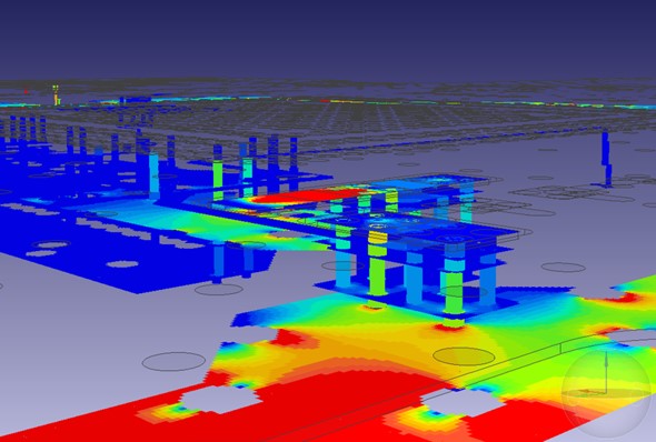
Mastering Early Detection in High-Speed PCB Design
Efficiency and reliability in high-speed PCB design demand early detection of signal integrity (SI), power integrity (PI), and electromagnetic compatibility (EMC) issues. These silent adversaries can compromise electrical performance. Screening for potential problems at the start of the design process is not just beneficial—it’s imperative.
The Imperative of Early Screening
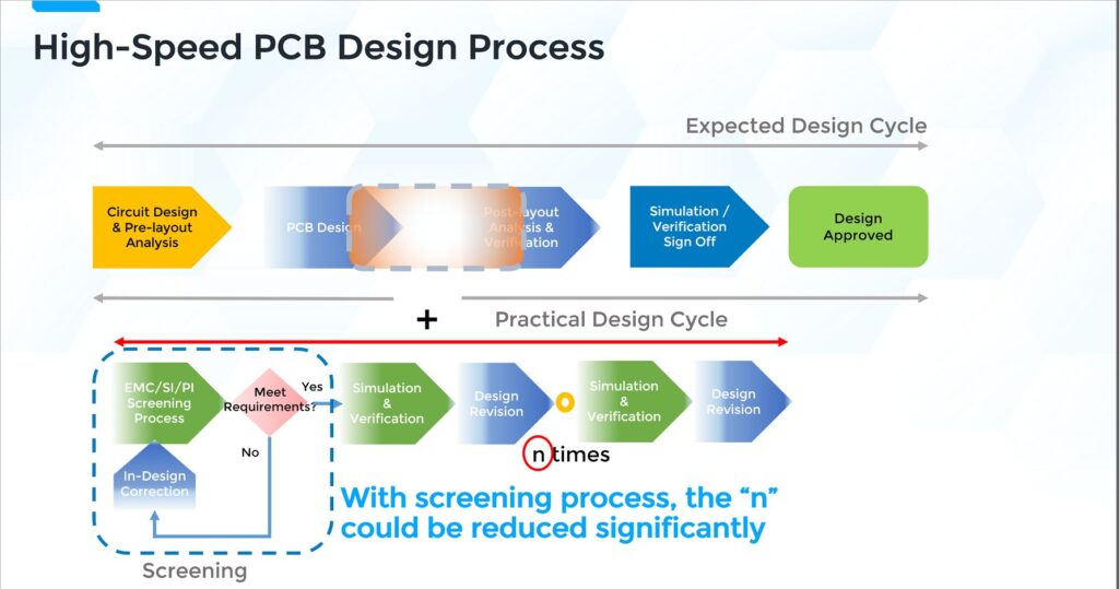
The mantra in high-speed PCB design circles is clear: the earlier, the better. Early screening processes are indispensable tools. They can detect subtle SI nuances that could derail a design or preempt EMC concerns that could lead to costly redesigns. Not only do they set the stage for robust design, but they also pave the way for significant cost reductions. In pursuing product development efficiency, skipping this crucial step could be akin to sailing without a compass.
Accelerating the Design Cycle
High-speed PCB design cycles are notoriously long and complex, often exacerbated by late-stage discoveries of SI/PI/EMC issues. Therefore, by incorporating screening at the initial stages of the design process, we can considerably shorten these cycles. Speeding up SI/PI/EMC validation is crucial as we push the envelope with designs geared toward handling speeds as staggering as 224 gigabits per second. Moreover, a thorough screening process can eliminate the need for backtracking—a significant time sink in the design cycle.
The Spectrum of SI Issues in High-Speed PCB Design
Signal integrity is not a singular challenge but a spectrum of potential pitfalls afflicting a high-speed PCB. Consequently, the advent of designs that cater to incredibly high-speed requirements has brought SI issues into sharper focus. These issues are not just about maintaining signal quality, but also about ensuring that the design can accommodate the rapid processing speeds expected of modern electronics. Therefore, SI validation, becomes a more elongated process, underscoring the importance of catching issues at the onset.
The Role of EDA Tools in SI Screening
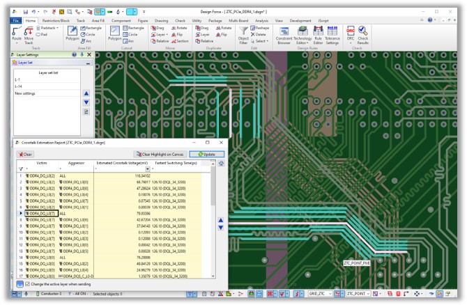
Effective early detection leans heavily on advanced Electronic Design Automation (EDA) tools. These tools must facilitate screening and be integrated into the design process, allowing for real-time corrections and iterations without the need to exit the design environment. Ideally, these EDA tools should include features like impedance calculators, topology templates, cross-talk estimation, power AC/DC quick screening and many SI/PI related conceptual fast check capabilities to support the designer in mitigating SI/PI issues from the get-go. More importantly, these screening features need to be in PCB design tools in order to have in-design corrections as needed.
Collaboration Between Design and Analysis
A robust screening process does not operate in isolation. It’s a collaborative endeavor between PCB designers, SI/PI/EMC engineers, and the tools they use.
The synergy between PCB design and analysis verification processes ensures that screening can be seamlessly followed by in-depth analysis. This collaboration is the cornerstone of a streamlined design process that can address conceptual issues before they snowball into significant hurdles.
The Future of Screening in PCB Design
As the complexity of high-speed PCBs grows, consequently, the need for comprehensive screening processes. Surveys suggest that prior screening can accelerate verification and sign-off processes by up to 50%. Thus, the question is no longer whether screening is necessary but rather how to implement it most effectively. It’s about ensuring the tools and methodologies are in place to detect and address SI/PI/EMC issues at the earliest conceivable point in the design process.
Conclusion: Early Detection as the Key to Success
High-speed PCB design efficacy hinges on the capacity to anticipate and resolve SI/PI/EMC issues swiftly. Addressing issues early in the design cycle is critical. As the industry moves towards increasingly complex and speedy designs, the role of early detection and screening processes becomes ever more critical. It’s about laying the groundwork for designs that are not just functional but are fine-tuned to perform optimally at the high speeds the modern world demands. By embedding early detection into the fabric of PCB design, engineers can ensure they remain ahead in a race where speed is everything.
Related Products and Resources
- Blog

- Blog
- Blog

- Blog
