Evaluation of System in Package Implementation Options in the Chiplet World
Cost-driven Decisions
Chiplets are emerging as an ever-growing choice for product development. The main factor in this chiplet implementation growth is cost. Development costs for new chip designs on 5nm nodes could soar as high as $600 million. This rapid cost increase often leads companies to pursue more cost-efficient options. With the chiplet path, a company can leverage the higher performance chip technologies where it makes sense. They can then leverage lower technology fab capabilities where performance is less critical. For instance, you can fabricate the processor via 7nm, and then fabricate the SRAM with a 14nm process. These tradeoffs allow the company to realize the most significant efficiencies for each element in its design.
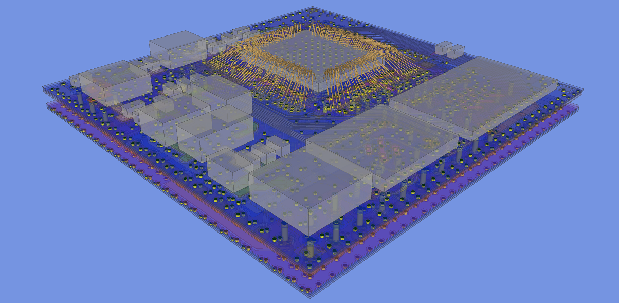
When deciding to separate the chips at fabrication, engineering must then merge them on a System in Package (SiP). This SiP becomes the critical merge point for these different functional elements. The System in Package implementation must realize the signal and power integrity requirements while also monitoring the cost-efficiency of the SiP fabrication. Typically, evaluating a chosen chiplet and SiP configuration happens after completing significant design work, leading to a great deal of engineering effort. This design flow can also lead to lengthy process delays if targets are unattainable with the chosen configuration. When that happens, engineers must implement changes and restart the design cycle. These iterative cycles add time and, ultimately, increase costs.
Cost vs. Performance
Product development teams need the ability to design with decision speed and cost vs. performance requirements in mind. With such a design flow, they will have the option to bring the chiplet bump pattern into the equation to configure the most routable and highest performance redistribution layer arrangement. At the same time, they can also factor in the SiP-level routability of the bump arrangement. Of course, if the chiplet configuration is already fixed, then the customer can leverage the SiP implementation flow for evaluations of various SiP configurations. These SiP configurations can include stacked die or through silicon via interposers if needed.
Speeding the Evaluation Process
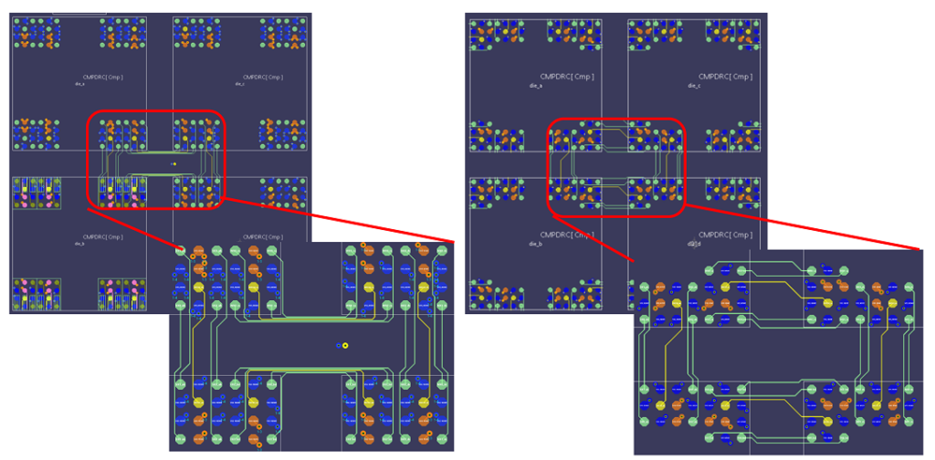
In partnership with one of our customers, Zuken performed an evaluation of two different bump patterns for a prototype chiplet using the following process:
- First, using a partial array of these patterns, we placed those to die onto a SiP.
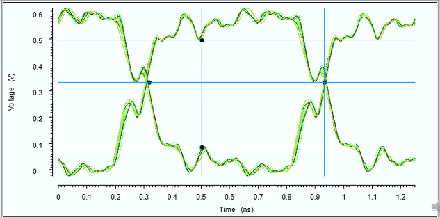
- Next, we examined the chiplet routing at the SiP level, focusing on routing length and signal integrity values. Through this examination at the SiP level, we determined that one configuration showed improvement over the other in length and signal quality.
- Lastly, we implemented the preferred configuration on the chiplet and incorporate it into the SiP.
This new evaluation process allowed the customer to quickly converge on a design configuration that met the targeted goals. Furthermore, it eliminated the need to evaluate the characteristics after considerable work on the final design. Therefore, in the end, the process helped the customer avoid scheduling delays, and the electrical performance exceeded targeted goals. These results bear a direct relationship too quickly evaluating various chiplet and SiP configurations and incorporating those results into the finalized design.
Summary
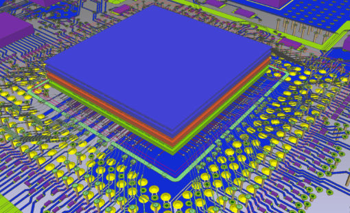
Zuken’s chiplet and System in Package implementation flow uses CR-8000 Design Force, the fastest, most effective multi-board PCB design solution available. By implementing this flow, customers are able to quickly evaluate various configurations of the SiP solution. These evaluation passes to ensure you’ll meet your SiP implementation cost and performance targets with minimal to no impact on the schedule.

-
Manager of Engineering Operations, SOZO Center at Zuken USA Inc.

- Blog

- Blog
- Blog

- Blog
Related Products & Resources
- Products
- Products
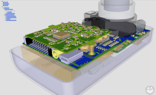
Design Force combines traditional 2D design with native 3D design and the latest human interface techniques, accelerated graphics and almost instantaneous rendering and refreshing. It is the fastest, most effective PCB design solution available today. Design Force enables design teams to layout their designs in the context of a complete system or product.

- Products
Building a competitive product today is much more difficult than a few years ago. Existing PCB-centric design processes are limited to a single PCB and do not provide the necessary tools for today’s competitive product development environment. PCB-centric design processes are falling behind.