In recent technology trends, 5G, IoT, super-computer, auto-driving car, robot, and artificial intelligence are popular words. However, the most popular one for PCB designs is “High-Speed” since the data speed transmission rate is already very high for electronic devices.
Due to the digital formation in the modern trends, “High-Speed” appears even more frequently for the product system designs.
What is High-Speed PCB Design?
In the digital world, we define speed as the speed at which one or more digital abstractions fail, as a direct consequence of the circuit speed.
For high-speed electronic designs, there are two types of circuit/device designs: Firstly, there are Analog (Microwave/RF) designs and secondly, there are Digital (Logic) designs. In analog designs, the speed is defined by the frequency of signals running inside the device. In digital designs, it’s a bit more complicated. Besides signal frequency, we also need to consider:
- Digital interpretation of analog values:
- Transistors as switches
- Analog voltages as “1” or “0” (logic)
- Logic devices as idealized Boolean primitives:
- Switches as logic elements
- Ignore the electrical characteristics of devices, wire, etc.
- Steady-state abstraction:
- Combinational: Outputs depend on inputs after a sufficient time
- Sequential: Outputs retain their settled state
So, the definition of the electronic design speed is:
- Signal frequency, for analog device design
- Signal rising/falling edge rates for digital device design
When the speed reaches the “high” level, the analog device design becomes microwave or radio frequency (RF) designs. The digital device design becomes a digital high-speed design through signal integrity analysis. Most PCB design issues are digital related in nature. Only a small portion of lower band RF designs use PCB materials directly. So let’s focus on high-speed digital design challenges here.
Typical Problems with High-Speed PCB Design
Typically, there are three problems when you are working on high-speed PCB design:
- Logic gates or flip-flops don’t have time to settle. When the buffer delay is too large compared to the speed, you’ll often see this happen.
- Clock skew causes racing. Having the clock and data signal in sync is essential for a parallel interface design. Any improper routing strategy could cause system failure when the speed is high.
- Wire (interconnect) acts like transmission lines. This is the most common issue when working with high-speed system designs. You will have to address the reflections due to the impedance mismatch, keeping in mind more than a simple lossless conductor connection.
All Wires are Transmission Lines
Usually, we discuss the transmission line theory when talking about microwave design and analysis. When we are talking about high-speed, we will have to use microwave theory to analyze a wire in the system. This will ensure that we treat the digital signal as an analog signal by looking into its detailed transitions.
Figure 1 Data net circuit
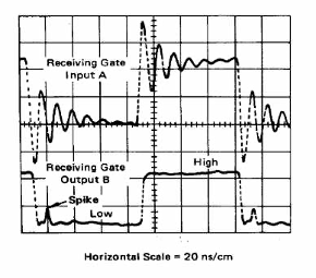
Figure 2: Signal waveforms on nodes A & B
In the past, signals on PCBs were slow. Thus, delays caused by wires were small compared with signal rising or falling times; wires passed digital voltages unchanged. Today, high-speed PCB design requires transmission line analysis because wire delays are long compared with signal rising or falling times. And wires don’t pass digital voltages unchanged.
How Fast is the High-Speed Signal on a PCB?
The speed of the signal is mainly defined by its rising/falling edge. It is also the ratio between the rising/falling time and the transition speed running through the wires.
The basic rule of thumb is that it will be considered a high-speed PCB if the delay on the wire is greater than ¼ of the rising/falling time. When this is the case, we will require additional analysis for signal integrity.
The following table shows examples requiring additional analysis where the signal rising/falling edge is 1 ns:
| Wire Type | Speed on Wire (inch/ns) | Wire Length (inch) | Wire Delay (ns) |
| Twisted pair | ~ 8.5 | > 2.125 | > 0.25 |
| Coaxial cable | ~ 8 | > 2 | > 0.25 |
| Microstrip (FR4) | ~ 7 | > 1.75 | > 0.25 |
| Stripline (FR4) | ~ 5.5 | > 1.375 | > 0.25 |
Does YOUR PCB require additional transmission line analysis?
What Happens when your Board Requires Additional SI Analysis?
There are many design challenges for high-speed PCB designs. Therefore, managing to solve the issues in the different design phases is a crucial step in the process. It can help you identify the best implementation strategy at the beginning, then mitigate errors in the end.
Here are a few phases that we should consider:
- Pre-layout analysis, In this phase, system and circuit designers will explore the best performance options and the highest cost-efficiency. This happens during the system design and circuit design (schematic) processes.
- Constraint-driven PCB design. In this phase, the PCB designer follows the constraint settings with specific high-speed routing functionalities.
- Post-layout verification. Once PCB layout is complete, this phase serves as quality assurance for signal integrity. Then, this is where you’ll run extensive simulations and multi-physics analysis.
Constraint-driven Methodology
Constraints serve as the messenger throughout the design process. They are consistent across all design phases and serve as a rule set, or a guideline, for PCB designs. However, a constraint-driven approach is different from a rules-driven approach. Constraint-driven methodology requires a truly unified design environment. Zuken’s CR-8000 Constraint Browser provides a single, unified interface for all constraint definitions and checks through schematic capture, PCB layout, and SI analysis. It adheres to a proven method to reduce design cycles and mitigate errors during the design process.
Conclusion
In modern technology trends, the data rate in electronic devices rises rapidly. This rise causes a series of challenges for high-speed PCB designs. Therefore, transmission-line analysis, advanced high-speed I/O buffer configuration, power delivery, EMI/EMC, etc., require greater focus.
Design analysis flow and phases are essential to ensure that the design process runs smoothly. The constraint-driven methodology enables a seamless transition process between the design phases. In my following blog posts, I’ll discuss detailed design flow and phases along with some specifics about high-speed design and analysis features in CR-8000.
Stay tuned!
References:
Related Products and Resources

- 2020 Technical Webinars
This webinar will explore a high-speed design process in CR-8000 that utilizes a constraint browser, topology template, crosstalk estimation, signal and power integrity simulations.

- 2020 Technical Webinars
In this session, we will review some of the new features that have been added in the CR-8000 Design Force and offer some explanation of how these additions will benefit our customers within their design flows.
- Products
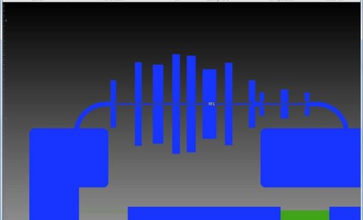
For a complete RF verification flow, CR-8000 Design Force interfaces with best-in-class, high-speed RF and electromagnetic analysis solutions.

- Webinar
The fast signal switching times of today’s digital systems require particular attention to the signal integrity during design to ensure reliable operation and EMI control.
