In consumer electronics, wearable technology is one of the most popular emerging areas in the last decade. Between popular devices such as smartwatches, fitness trackers, VR headsets, or even medical devices, wearables seemingly permeate every aspect of our daily lives.

Like all revolutionary new products, wearable electronics are only possible due to innovations in the underlying technology. Specifically, innovations in printed circuit board (PCB) design and technology are a major enabler in the rise of wearable devices.
In this post, we’ll explore the role of PCBs in wearable technology, PCB innovations that have benefited the wearable industry, and how Zuken’s CR-8000 software lies at the heart of this revolution.
The Role of PCB Design for Wearable Technology
PCB design is the backbone of any electronic device, and wearable technology is no exception. PCBs provide the necessary platform for mounting and interconnecting the various electronic components that make up these devices. However, PCB design for wearable technology presents unique challenges and design tradeoffs that don’t exist in other fields.
For example, wearable devices must simultaneously be small, comfortable, low-power, aesthetically pleasing, and durable. To accommodate all of these needs, the PCBs in these devices must be compact, lightweight, and flexible to fit into various forms and shapes. Additionally, they must be robust enough to withstand physical stress and exposure to elements like sweat and moisture. Power efficiency is also necessary, as wearable devices often rely on small batteries with limited capacity.
Ultimately, PCB design for wearable technology is a delicate balance between functionality, form factor, and power efficiency. Balancing these needs requires innovative approaches and advanced design tools.
Innovations in PCB Design for Wearables
Several innovative design techniques have emerged to meet these challenges. Here are a few key advancements:
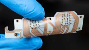
Flexible and Stretchable PCBs: Traditional rigid PCBs are not suitable for wearables that conform to the human body’s shape. Flexible and stretchable PCBs, made from materials like polyimide, are a game-changer in this regard.
- High-Density Interconnect (HDI) PCBs: HDI technology allows for a higher density of components on a PCB, making the devices smaller and more efficient. This is crucial for wearable devices where space is at a premium.
- Advanced Power Management: PCB innovations often focus on improving power management. This includes techniques for reducing power consumption and improving battery life, which are critical for wearable devices.
Zuken’s CR-8000: Aiding the Wearable Revolution
As the wearable technology industry continues to grow, so does the need for advanced PCB design tools. Zuken’s CR-8000 is a product-centric design solution that delivers the capabilities to design the next generation of high-tech wearable devices.
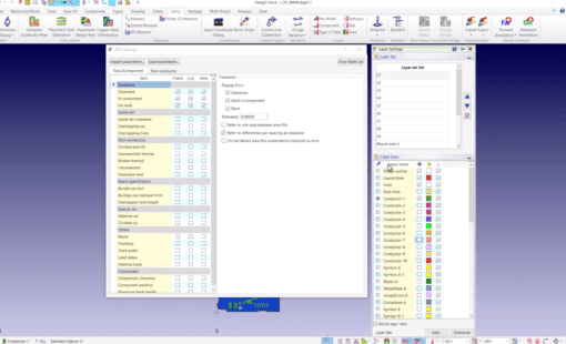
One benefit of the CR-8000 tool is its ability to facilitate collaboration. Specifically, CR-8000 provides a fully integrated environment for system-level design, allowing seamless collaboration between mechanical and electrical design teams. Its advanced capabilities, including 3D layout, design, and MCAD co-design, make it an ideal tool for designing complex wearable devices.
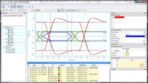
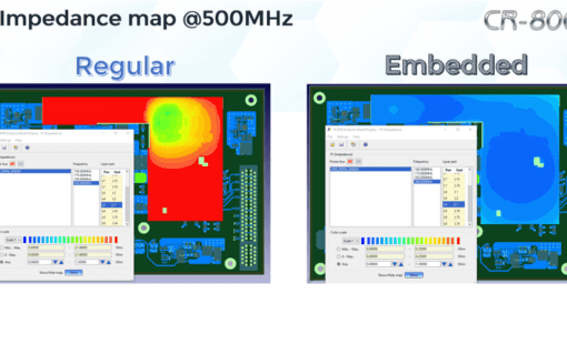
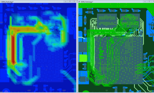
Moreover, CR-8000’s power integrity analysis and thermal simulation capabilities ensure that wearable devices are not only compact and lightweight, but also reliable and efficient. By enabling designers to identify and resolve potential power and thermal issues early in the design process, CR-8000 accelerates the advancement of wearable technology.
Continued innovations in PCB design, coupled with advanced design tools like Zuken’s CR-8000, are driving the wearable technology revolution. As we continue to push the boundaries of what’s possible, we can look forward to even more exciting developments in this field.
Related Products and Resources

- Blog
- Blog

- Products
Building a competitive product today is much more difficult than a few years ago. Existing PCB-centric design processes are limited to a single PCB and do not provide the necessary tools for today’s competitive product development environment. PCB-centric design processes are falling behind.


