Optimizing PCB Performance with Embedded Capacitance
The drive for greater efficiency has led to significant innovations in printed circuit board (PCB) design. Among these, embedded capacitance stands out as a game-changer, offering numerous advantages over traditional decoupling capacitor approaches. This post explores how embedded capacitance technology enhances PCB performance to meet the high demands of modern electronics.
The Challenges of Power Delivery in Modern PCBs
PCB designers constantly face the challenge of managing power integrity, especially as devices become faster and more compact. The traditional method of using discrete decoupling capacitors is becoming less feasible due to space constraints and the inherent limitations in their ability to handle higher speeds effectively.
Embedded capacitance technology (ECT) addresses these challenges by integrating the capacitor function directly into the PCB layers. This integration saves space while significantly improving electrical performance by reducing the inductance and resistance paths that affect signal integrity and power quality.
What is Embedded Capacitance?
Embedded capacitance technology (ECT) integrates capacitance directly into PCBs or chip packages to meet demands for miniaturization and improved electrical performance. Emerging in the late 1990s, this technology replaces traditional surface-mounted capacitors to overcome limitations in physical size and enhance performance, especially in high-frequency applications. ECT uses a dielectric material sandwiched between conductive layers within the PCB, significantly increasing capacitance per unit area and optimizing the electrical properties essential for modern electronic devices.
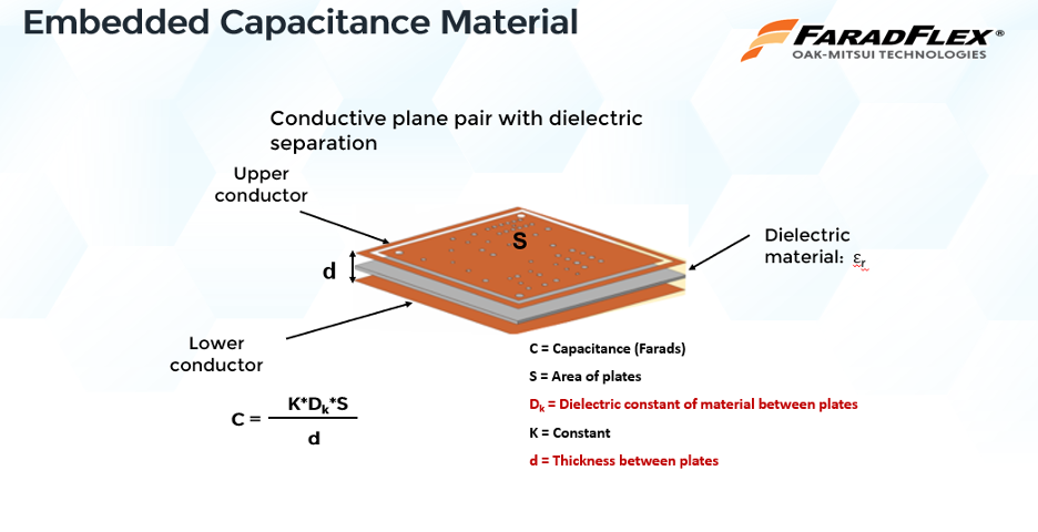
Embedded Capacitance Materials
ECT uses ultra-thin, high-dielectric constant materials between the planes to create high capacitance. The dielectric material acts as the capacitor’s insulator, while the surrounding copper layers act as plates. This configuration allows for a much higher capacitance per unit area than traditional FR-4 materials. It also brings the benefits of lower impedance and inductance for the plane pairs.
Advantages of Optimizing Performance
Enhanced Power Integrity
Using embedded capacitance can drastically reduce the number of discrete capacitors needed on a board. This reduction simplifies the board layout and frees up space for other critical components or functionality. Moreover, ECT provides a more stable power supply, which is crucial for high-performance electronics sensitive to power fluctuations.
Improved Signal Integrity
Signal integrity is paramount in high-speed PCB designs. Embedded capacitance helps maintain signal integrity by minimizing the loop inductance and providing a more stable impedance profile across a wide frequency range. This stability is vital for achieving high-speed data transmission without significant losses or errors.
Cost and Reliability Benefits
Incorporating embedded capacitance can lead to cost savings in material and assembly processes. By reducing the number of components, the assembly time and the potential for soldering errors decrease, thereby enhancing the reliability of the final product. Additionally, the inherent properties of embedded materials can lead to longer-lasting and more robust boards.
Implementing Embedded Capacitance in PCB Design
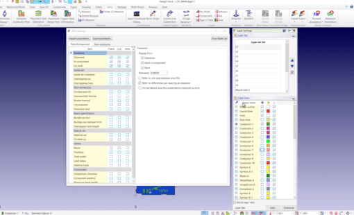
When implementing ECT, follow these steps:
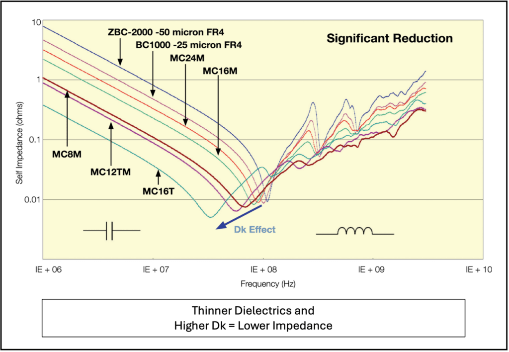
- First, replace the pair of planes that you are aiming to enhance. It needs to change the layer stack using the embedded capacitance material specifications. Let’s use FaradFlex material MC12TM as an example: Dielectric layer thickness: 0.012mm; Dk(Dielectric Constant): 10.0; Df(Loss Tangent):0.015
- Next, in the simulator, determine the total plane pair capacitance. The CR-8000 Analysis Module automatically displays this information on the PI page.

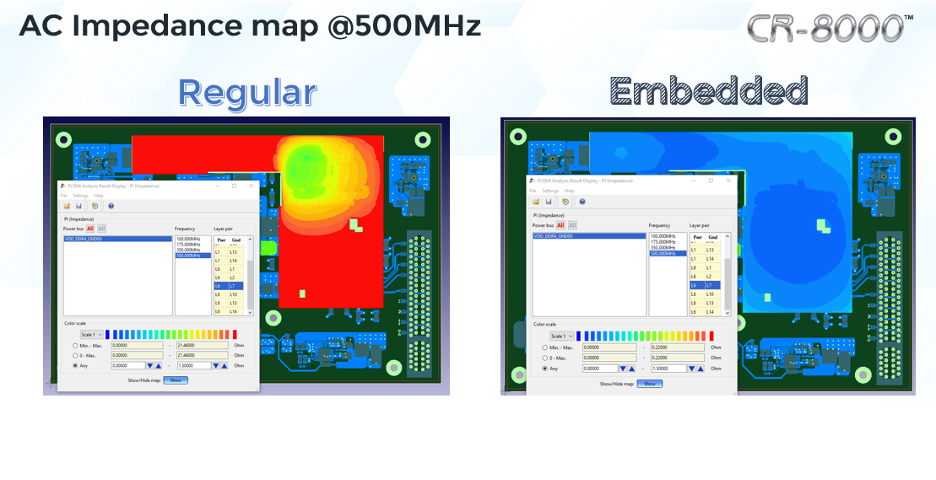
Plane Pair Total Capacitance - Finally, find the results for impedance spectrum and impedance color mapping using CR-8000 PI simulations. You also can compare the results with or without embedded capacitance materials if you have stored the previous simulation result, as shown in the pictures below:
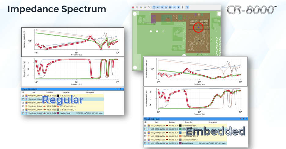
Impedance Spectrum
Adopting embedded capacitance requires careful consideration of the design and materials used. Design tools like the CR-8000 from Zuken facilitate the integration of these technologies by allowing designers to simulate and analyze the impacts of embedded capacitance before physical prototypes are built. This capability is crucial for optimizing the design process and ensuring that the benefits of embedded capacitance are fully realized.
Conclusion
Embedded capacitance in PCB design is not just a trend but a substantial shift in how boards are designed and manufactured. As the electronics industry continues to push the boundaries of what’s possible, technologies like embedded capacitance are critical in overcoming the limitations of traditional designs and opening up new possibilities for innovation and performance.

- Blog

- Blog

- Blog

- Blog
Related Products and Resources
- Blog

- Blog
- Blog