When you venture into electronics and circuitry, you soon find the Printed Circuit Board (PCB) at the heart of most modern devices. If you’ve looked inside an electronic device, you’ve noticed the PCB: that green or blue board dotted with lines and components. Let’s dive into the PCB design basics to understand the significance of this board.
What is a PCB?
A Printed Circuit Board (PCB) mechanically supports and connects electronic components using conductive tracks, pads, and other features. Engineers etch these features from copper sheets and laminate them onto a non-conductive substrate. However, this describes the traditional construction of the PCB. Specialized applications might also use a flex PCB. We’ll delve into that later.
Methods of PCB Design
As you delve into PCB design basics, you find three primary design methods:
Where it All Began: Designers drew the initial schematics by hand and crafted the PCB artwork using tape on mylar. Despite requiring much effort and being prone to errors, this method paved the way for computer-aided designs.
Computer-Aided Design (CAD): This method revolutionized PCB design, spawning a new industry. With specialized software, designers draw schematics, position components, and route traces with precision. CAD software provides error-checking, simulation, and tools for generating manufacturing files, making the design process more streamlined.
Auto-Routing: As designs grew, manually routing connections became tedious. Designers developed autoroutes to route connections, adhering to specific rules quickly. While some designers manually route critical paths for better control, auto-routing accelerates the process.
The project’s complexity, available tools, and personal preferences often determine your method choice. Most PCB designers combine CAD and manual techniques for the best outcomes.
Starting with the Schematic
Before you delve into the PCB layout, you need to create the PCB’s logical representation – the schematic. A schematic diagram lists the components, connectors, and pin-to-pin connections. The CAD tool then moves the schematic or logical representation to the PCB layout tool for physical design. Every PCB project starts with a schematic.
Choosing the Right Components
Choosing components is a lengthy phase of schematic creation. Modern components come in various shapes, sizes, and functions. The appropriate component offers the required functionality while being economical and accessible. Supply chain factors also influence component selection.
PCB Footprint and Layers
Before transitioning to the PCB layout, you must define the PCB shape and layer stack. If the PCB needs to fit inside an enclosure, the mechanical team dictates the PCB’s shape and mounting hole locations. The layer stack or stackup indicates the board’s routing surfaces. Depending on the design’s density, these can vary from one to over 24.
Power and Ground Planes
Most multi-layered PCBs have dedicated power and ground layers. These layers supply power to components, assist in heat dispersal, and maintain signal integrity.
Component Placement
After establishing the PCB shape and stack up, the placement of components begins. PCBs generally follow a logical sequence, suggesting component placement. Mechanical requirements might dictate the positions of certain components, like connectors. Proper component placement is crucial for the project’s overall success.
Routing the Board
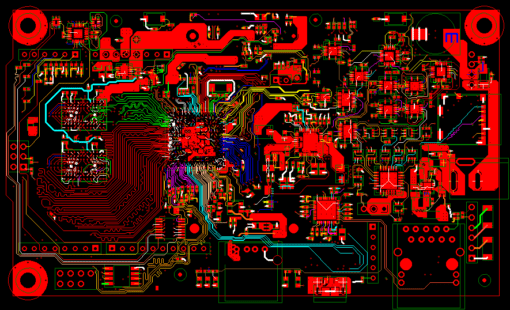
After placing the components, you then “route” the board. You must make the pin-to-pin connections specified in the schematic in the real world. We call the copper connection on the board a trace. The holes on the board, which allow the trace to move between layers, are called vias. Autoroutes can make routing much quicker than manual efforts.
Setting the Design Rules
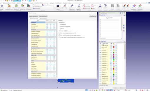
Most PCB design software allows you to set design rules. These rules ensure your PCB design meets specific standards like trace width, spacing, and hole dimensions. Adhering to these rules prevents manufacturing errors and ensures PCB reliability.
Finalizing the Design with a Design Rule Check (DRC)
After finishing component placement and routing, running a Design Rule Check (DRC) is vital. This check confirms that your design matches the set criteria and identifies any overlooked errors.
Manufacturing the PCB
You generate manufacturing files to cut, drill, and etch the raw board with copper. File formats have changed over time. We started with Gerber files, but IPC-2581 is the prevailing standard now. After fabricating the board, assembly starts. This step involves positioning the physical components on the board and soldering them to the right spots. Pick-and-place machines have now replaced the manual process, speeding things up immensely.
Prototyping and Testing
Before jumping into mass production, consider making a PCB prototype. Testing this prototype ensures everything operates correctly, allowing you to make necessary adjustments.
Zuken’s Solutions for PCB Design
Zuken stands out in the electrical and electronics design domain, offering cutting-edge solutions for today’s design challenges.
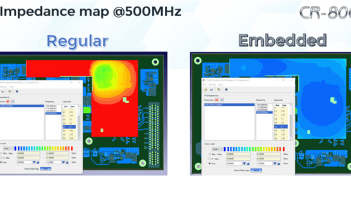
CR-8000: Zuken’s flagship product, CR-8000, provides a PCB subsystem 2D/3D design platform. It covers the entire PCB design process, ensuring superior quality and reliability for complex tasks. It also supports integrated IC packaging.
eCADSTAR: A contemporary PCB design tool for the broader market. eCADSTAR marries an intuitive interface with 3D design and internet-connected libraries, enhancing schematic capture and layout.
DS-CR: Zuken’s DS-CR is a data management platform for companies focusing on project management, change management, multi-site libraries, and PLM integration. DS-CR ensures efficiency and quality in PCB design, catering to various design complexities and hurdles.
Conclusion
Though mastering PCB design basics might appear overwhelming initially, current PCB tool options simplify and optimize the process. As electronic products shrink and gain power, the PCB remains central to every advanced product.
Related Products & Resources
- Products

- Products
Today’s Desktop PCB Design tools require better connectivity to the outside world. eCADSTAR offers a newer level of connectivity that brings users closer to their parts providers than ever before. This allows Engineers to selected parts and drag them directly to their design. Add the additional functionality of high power Signal integrity verification and Power integrity analysis and you have the Ultimate Desktop PCB Engineering solution.
- Products

- Products
Building a competitive product today is much more difficult than a few years ago. Existing PCB-centric design processes are limited to a single PCB and do not provide the necessary tools for today’s competitive product development environment. PCB-centric design processes are falling behind.
