Introduction to RF PCB Routing Techniques
Welcome to our discussion on RF PCB signal routing in PCB design, where technique and precision play pivotal roles in signal integrity. This post examines the debate between using curved bends and mitered or chamfered corners in RF routing design. We use modern PCB design tools and advanced simulations to reveal how different bending techniques impact signal loss, impedance, and overall circuit performance under various frequency ranges. Join us as we navigate the intricacies of RF PCB routing to achieve optimal design outcomes.
The Technological Shift in PCB Design
In RF PCB routing, controlling impedance and capacitance ensures that maximum power reaches the end of a route. It is no secret to RF engineers that meeting the route requirements is crucial to the design’s success.
This critical aspect of RF engineering has evolved from manual hand-taping methods to sophisticated CAD-based techniques. Modern PCB design tools now enable designers to apply precise calculations to create bends with controlled radii, enhancing the design’s efficiency and effectiveness.
Evaluating Bends in RF PCB Routing
One technique was, and still is, to miter the corners of a 90-degree angled trace. This helped to stabilize the capacitance at the corners and prevent impedance drops. The guidelines were rules of thumb but easy to meet using a razor knife. However, RF PCB routing now benefits from the ability to create perfect radius bends using modern tools, bypassing older methods that relied on less precise techniques.
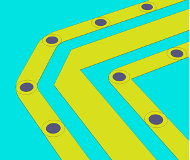
I often wonder why designers using modern PCB design tools still use this method. A simple calculation, radius = 3x trace width, helps to determine the optimal bend radius or sweep in the route, though it does not consider the operating frequency.
Once the bend radius is established the route can be free of solder mask, shielded, and surrounded by vias to create a nearly perfect ground return path. Decades ago, creating a perfect radius using tape was almost impossible.

The Role of Modern CAD Tools in RF Design
The introduction of the 3D field solver transformed RF PCB routing by allowing RF engineers to replace assumptions with accurate, science-backed designs. We recently used ANSYS SIwave Q3D to extract s-parameters (lossy) and verify the optimal scenario for RF PCB routing under 30GHz. The results highlighted the advantages of newer bending techniques over traditional methods, especially in higher frequency ranges.
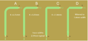
- We generated a simple PCB design and routed four tracks using three different radius turns and a 45-degree chamfer turn for RF signals.
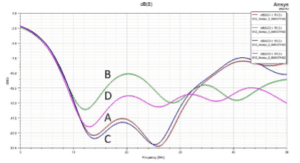
- The results for dB Loss were obvious.
- Under 10 GHz, all tracks showed a consistent loss.
- Within 10-30 GHz, the best is case B. The second best is case D (45-degree miter), while cases A and C are equally worse. Overall, cases B and D showed consistent results over 10-50GHz.
Practical Insights from Simulated Scenarios
We simulated four routed tracks using three different radius turns and a 45-degree chamfer turn for RF routes. These tests demonstrated that under 10 GHz, all tracks maintained consistent loss levels. However, from 10-30 GHz, certain designs performed significantly better, showcasing the importance of choosing the right bending technique in RF PCB routing for higher frequencies.
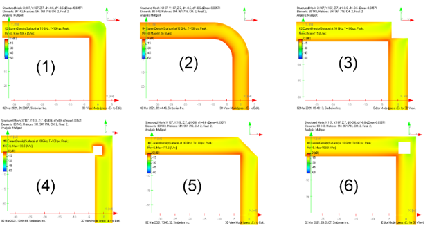
We referenced an article published by Dr. Yuriy Shlepnev. (23) How Interconnects Work: Minimal-reflection 90-degree bends in strip lines | LinkedIn
The article suggests additional patterns that are difficult to create using a modern PCB design tool, however examples 2 and 5 remain the common methods for consistent results. I encourage you to read the entire article, and then bookmark it.
In 2024 we should be using the PCB design tools for the accuracy they provide and not using them to mimic manual techniques from decades past.
Insights from Gemini on RF PCB Routing: Mitered Bends vs. Arcs
While running these tests ourselves, we thought it might be fun to consult Gemini (Google AI) to see the results. We asked the following question:
Whenever possible RF traces should use 45° mitered bends instead of arcs. Is this correct?
The response from Gemini:
- It’s not entirely accurate to say that mitered bends are always preferable to arcs in RF applications. Both have their pros and cons, and the optimal choice depends on several factors. Here’s a breakdown:45° Mitered Bends: These are sharp, angled turns where the trace is cut at a 45-degree angle to create the bend.
- Arcs: These are smooth, curved transitions between trace segments.
Mitered bends vs. Arcs:
- Radiation: Both mitered bends and arcs are generally better than sharp 90-degree bends for reducing radiation. However, arcs still have an advantage due to their smoother transition.
- Impedance Control: Mitered bends can introduce some impedance variations compared to arcs, but it’s generally less severe than multiple sharp bends.
So, when are mitered bends a good choice?
- Space Constraints: When space is extremely limited, mitered bends allow for tighter routing compared to arcs.
- Lower Frequencies: At lower frequencies, the impact of radiation and impedance variations from mitered bends is less significant compared to higher frequencies.
Here are some additional points to consider:
- Controlled Impedance Mitered Bends: Some advanced design software might offer options for creating mitered bends with controlled impedance profiles. However, this is not as common as controlled impedance arcs.
- Manufacturing Considerations: Mitered bends can be slightly more challenging to manufacture compared to arcs, especially on very thin traces.
Overall:
- Arcs are generally preferred for their superior performance in minimizing radiation and maintaining consistent impedance.
- Mitered bends can be a good alternative when space is a critical constraint, especially at lower frequencies.
For the best approach:
- Consider the specific requirements of your design, including frequency, signal integrity needs, and space limitations.
- Consult your PCB design software’s capabilities for creating controlled impedance features, whether arcs or mitered bends.
- Refer to resources on RF layout techniques for detailed guidance on trace routing practices.
Advancing PCB Design with Modern Tools
While traditional chamfering techniques will get the job done, using a calculated curved bend with modern PCB design software offers superior control over signal clarity and impedance, especially as operating frequencies increase. Embracing these advanced RF PCB routing techniques will be crucial in meeting the demands of increasingly complex electronic designs. Harnessing the full potential of CAD tools allows for more precise and effective RF PCB routing, ensuring that our designs keep pace with technological advancements and industry needs. In short; In 2024, we should be using the PCB design tools for their accuracy and not to mimic manual techniques from decades past.
*Special thanks to Lance Wang of Zuken USA for his input.
Related Products and Resources

- Blog
- Blog
- Blog

- Blog

