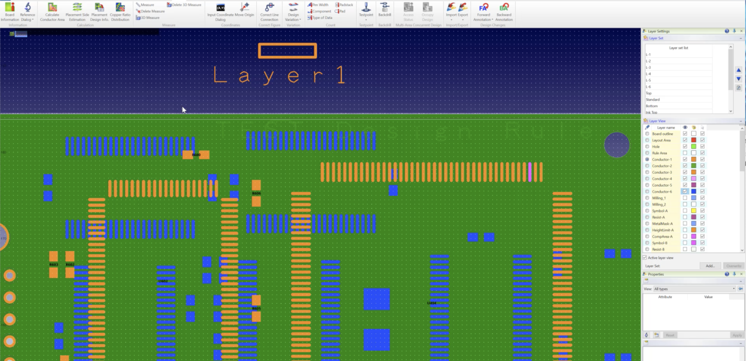
Board design rule checks only check up to the board outline. If you had dropped or moved some data outside the board outline there was no check for this until now. Checking for data outside the board area can now be done using the [Data outside Board] tool in Design Force 2020.
On the ribbon, click [Utility] – [Information] – Board Information [Board Information].
The [Board Information] dialog is displayed.
Check [Data outside Board] on the [Board Information] dialog and click [Browse]; the following information is displayed.
Figure layers and coordinates outside the board outline
Only the figures separated from the board outline can be detected by specifying [Offset value] using the [Advanced] button.
The target objects are as follows:
- Line
- Area fill
- Meshplane
- Area
- Character
- Component symbol
- Pad
- Padstack
- Round hole
- Slot Hole
- Rectangular Hole
- Rule area
- Remarks
Only visible layers are targeted for detection.
The drawing layers are not targeted for detection.
- Products
Zuken reveals details of release 2020 of its advanced 3D multi-board EDA environment CR-8000.
- Products
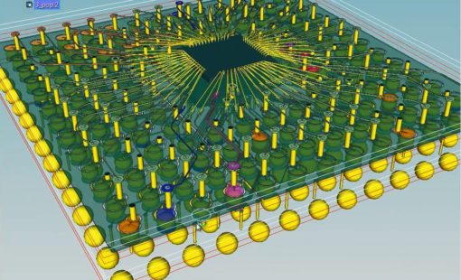
Design Force offers an intuitive, integrated environment for designing single and multi-die packages for wire-bond, flip-chip, and high density advanced packaging. Designers can start designs with early prototype input of chip and package data from the library, reuse data from IC layout tools, and take advantage of parametric wizards to streamline the creation of the system
- Products
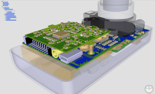
Design Force combines traditional 2D design with native 3D design and the latest human interface techniques, accelerated graphics and almost instantaneous rendering and refreshing. It is the fastest, most effective PCB design solution available today. Design Force enables design teams to layout their designs in the context of a complete system or product.

- Products
Building a competitive product today is much more difficult than a few years ago. Existing PCB-centric design processes are limited to a single PCB and do not provide the necessary tools for today’s competitive product development environment. PCB-centric design processes are falling behind.
