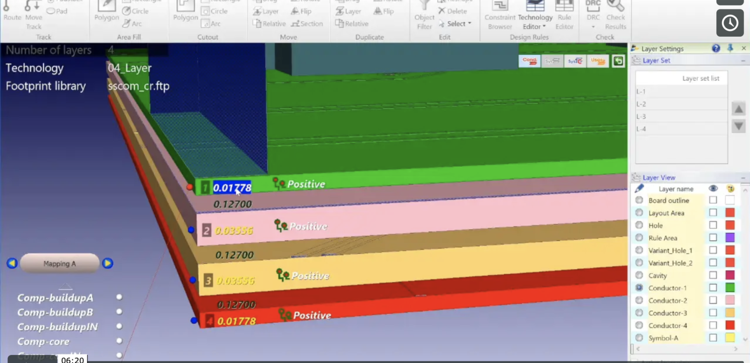
In Design Force you can edit your board Technology using the 3D Technology Editor. In the 3D technology edit window, you can perform the following operations to edit the technology for the board.
“Adding or Deleting a Conductor Layer to/from a Board (3D)”
“Adding or Deleting a User Defined Layer to/from a Board (3D)”
“Editing Layer Attributes of a Board (3D)”
“Editing the Layer Mapping of a Board (3D)”
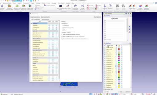
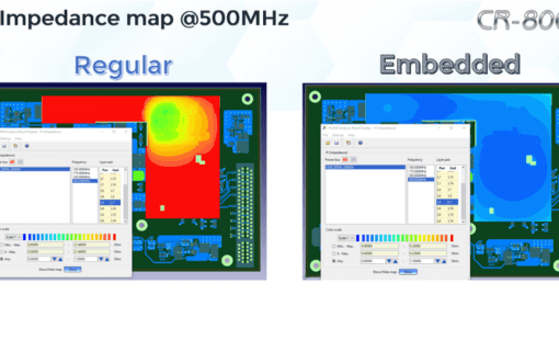
In the video, I also use the 2D Technology Editor to edit the displayed layer order and comments. I also edit the board configuration in the Rule Editor to make sure my design is ready for the simulation tools.
Related Products and Resources

- Products
Today’s Desktop PCB Design tools require better connectivity to the outside world. eCADSTAR offers a newer level of connectivity that brings users closer to their parts providers than ever before. This allows Engineers to selected parts and drag them directly to their design. Add the additional functionality of high power Signal integrity verification and Power integrity analysis and you have the Ultimate Desktop PCB Engineering solution.
- Products
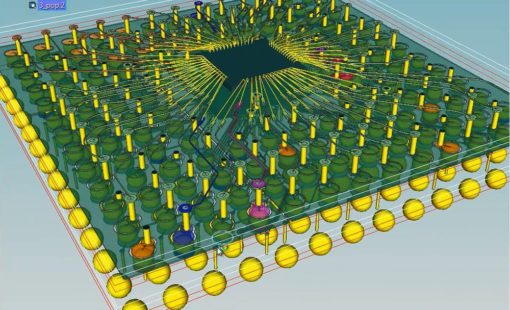
Design Force offers an intuitive, integrated environment for designing single and multi-die packages for wire-bond, flip-chip, and high density advanced packaging. Designers can start designs with early prototype input of chip and package data from the library, reuse data from IC layout tools, and take advantage of parametric wizards to streamline the creation of the system
- Products
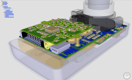
Design Force combines traditional 2D design with native 3D design and the latest human interface techniques, accelerated graphics and almost instantaneous rendering and refreshing. It is the fastest, most effective PCB design solution available today. Design Force enables design teams to layout their designs in the context of a complete system or product.

- Products
Building a competitive product today is much more difficult than a few years ago. Existing PCB-centric design processes are limited to a single PCB and do not provide the necessary tools for today’s competitive product development environment. PCB-centric design processes are falling behind.
