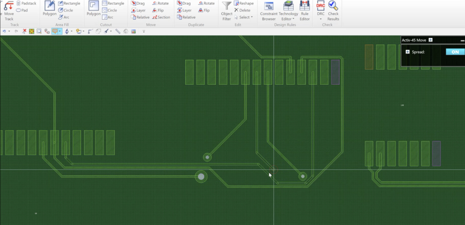
A function that pushes tracks away and avoids obstacles when a via is moved has been added. This is a great advantage for the designer when routing. What use to take a lot of time to move traces and vias to move a via to a new location has been greatly enhanced using the “Activ-45 Router”.
Move a via while surrounding routing patterns are pushed away. If the track pushed away is an obstacle, it is circumvented.
On the ribbon, click [Home] – [Track] – [Move Track] to start the Move Track command.
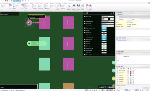
On the command dialog, set [Activ-45 Move] to [ON].
Select the target object.
On the canvas, move the cursor in the direction of movement.
Specify a destination on the canvas.
The routing pattern is moved while the connection is kept.
The target objects are as follows:
- Padstacks (excluding in-component and edited padstacks)
Assist menu
The following assist menu items can be selected by right-clicking the mouse:
The following video will show a quick demonstration of this:
Read more of our Tech-Tips here!
Learn more about Zuken’s CR-8000 Design Force!
Related Products and Resources

- Products
Today’s Desktop PCB Design tools require better connectivity to the outside world. eCADSTAR offers a newer level of connectivity that brings users closer to their parts providers than ever before. This allows Engineers to selected parts and drag them directly to their design. Add the additional functionality of high power Signal integrity verification and Power integrity analysis and you have the Ultimate Desktop PCB Engineering solution.
- Products
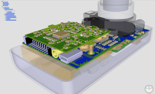
Design Force combines traditional 2D design with native 3D design and the latest human interface techniques, accelerated graphics and almost instantaneous rendering and refreshing. It is the fastest, most effective PCB design solution available today. Design Force enables design teams to layout their designs in the context of a complete system or product.

- Products
Building a competitive product today is much more difficult than a few years ago. Existing PCB-centric design processes are limited to a single PCB and do not provide the necessary tools for today’s competitive product development environment. PCB-centric design processes are falling behind.
