Engineers sometimes like to know which nets are routed on each conductive layer separately. They also like to know the total trace length and via count for each net for all the conductive layers for the PCB. There is a quick and easy way to do this in CR-8000 Design Force.
The following steps will need to be done:
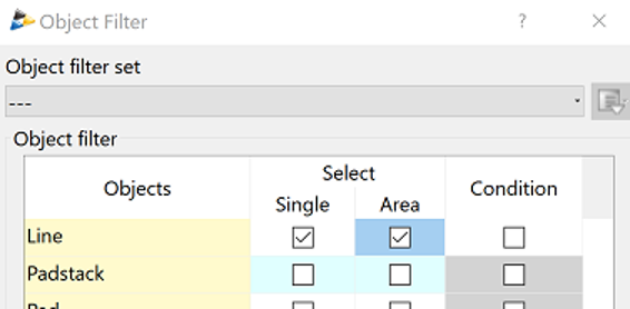
1. Create an Object Filter in Design Force to select only “Line”
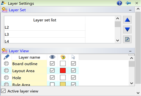
2. Set “Layer Settings” to show only “Active Layer” by checking the box, all other conductive layers can be set to “Not Displayed”.
3. Turn on “Select Only Active Layer” ![]() on the bottom Status Bar.
on the bottom Status Bar.
4. Turn on “Auto Sending” ![]() on the bottom Status Bar.
on the bottom Status Bar.
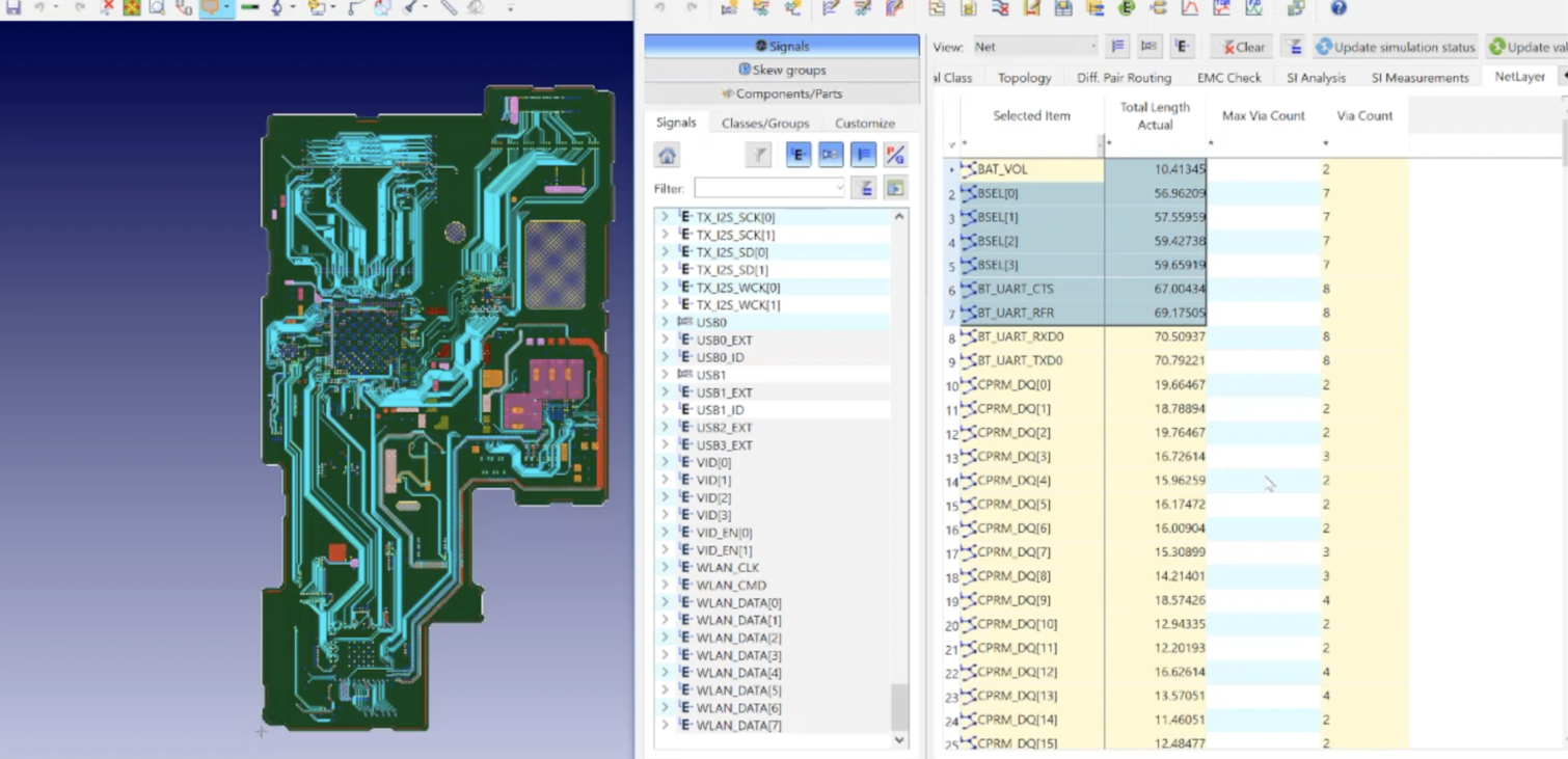
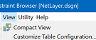
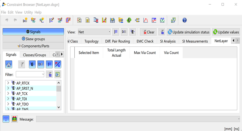
5. Open Constraint Browser and set up as shown below. You will notice I made a custom tab called “Net Layer” this can be done under View->Customize Table Configuration…
6. Make sure “Send Selected” ![]() is turned on.
is turned on.
7. Before you begin “Reconstruct E-net”![]() .
.
8. Set “View” to Net.
9. After frame Selecting each Active Layer “Update values”
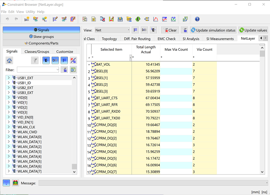
10. The following is an example of Conductor 3 nets displayed in Constraint Browser.
NOTE: If you want to add the “Z” length of the via to the “Total Actual Length” you will need to check the box “Include via length in Z-direction” Under File -> Configuration->Advanced.

The following video will show a quick demonstration of this:
Related Products & Resources

- 2020 Technical Webinars
In this session, we will review some of the new features that have been added in the CR-8000 Design Force and offer some explanation of how these additions will benefit our customers within their design flows.
- Products
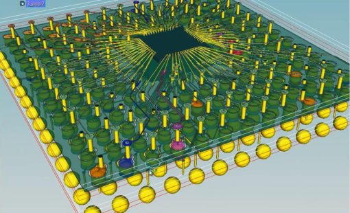
Design Force offers an intuitive, integrated environment for designing single and multi-die packages for wire-bond, flip-chip, and high density advanced packaging. Designers can start designs with early prototype input of chip and package data from the library, reuse data from IC layout tools, and take advantage of parametric wizards to streamline the creation of the system
- Products
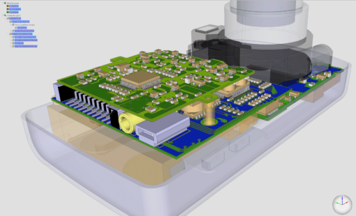
Design Force combines traditional 2D design with native 3D design and the latest human interface techniques, accelerated graphics and almost instantaneous rendering and refreshing. It is the fastest, most effective PCB design solution available today. Design Force enables design teams to layout their designs in the context of a complete system or product.

- Products
Building a competitive product today is much more difficult than a few years ago. Existing PCB-centric design processes are limited to a single PCB and do not provide the necessary tools for today’s competitive product development environment. PCB-centric design processes are falling behind.
