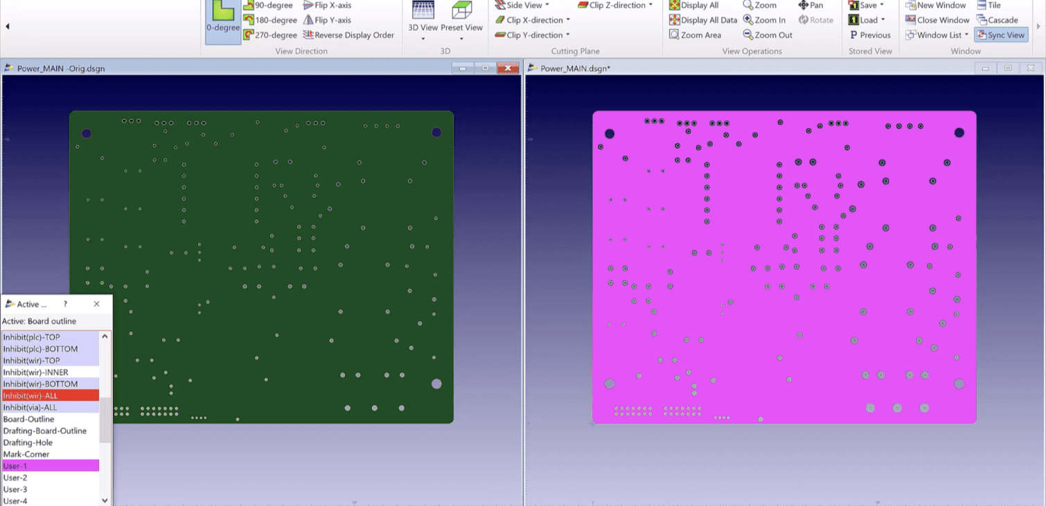
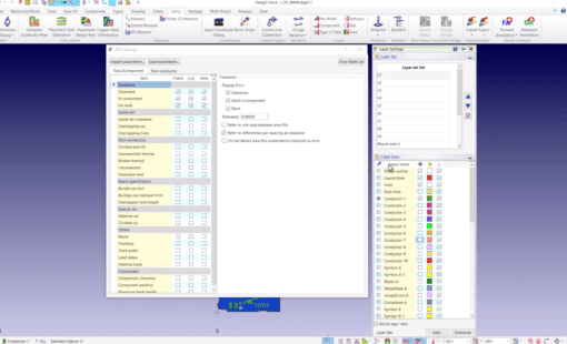
When designing PCBs, ensuring there’s no copper foil in the resist openings is crucial for the overall functionality of the board. One of the most effective ways to check this is by switching to a positive view of the solder resist layer in your CR-8000 Design Force software rather than sticking with the conventional negative view.
Why Switch to Positive View in CR-8000 Design Force?
By viewing the resist layer in its positive/negative reversed display, designers can get a clearer picture of potential issues. Additionally, this unique CR-8000 Design Force procedure makes verifying your PCB design much easier and more efficient.
Benefits of Positive Resist Layer View in CR-8000 Design Force:
- Enhanced clarity when checking for copper foil in resist openings.
- Alternative design verification process.
- Positive visualization of the resist layer.
Step-by-Step Guide to Switching to Positive View in CR-8000 Design Force:
- Initiate active layer view by turning off visibility for all layers.
- Set the board outline layer as your active layer.
- Activate a user-defined layer by generating an offset figure.
- With the resist layer active, use the subtract figure to encompass the entire board.
- Right-click and select Selection End.
- Your user-defined layer will now positively showcase the resist layer, making the checking process more efficient.
The Importance of a Reliable Design Check:
In the world of PCB design, attention to detail is vital. CR-8000 Design Force’s Positive Solder Resist View offers another way of viewing negative data. This method can reveal exposed copper that may otherwise lead to manufacturing issues. By utilizing the positive solder resist view, designers ensure top-notch designs and avoid costly errors. The advantages of this efficient verification process stand out, especially in a competitive market.
For a visual demonstration, please refer to our video tutorial below.


