The traditional use of through-hole vias is well-known in PCB design, especially within the CR-8000 Design Force tool. However, designers face new challenges as technology evolves and designs become more intricate and compact. One effective solution is the implementation, a technique that can revolutionize your PCB design process. This blog post covers the specifics of setting up buried vias in Design Force, offering a step-by-step guide to optimize your PCB design.
Understanding the Need for Buried Vias
The Challenge with Conventional Vias
When designing a PCB with Design Force, the standard approach involves using through-hole vias. However, as designs get more complex and space is at a premium, fitting all the necessary devices and routing paths on the board becomes more challenging. This is where the concept of buried or blind vias comes into play.
Advantages of Buried Vias
Buried vias offer a crucial advantage – they free up design space for routing. They are particularly beneficial in compact PCB designs where every millimeter counts. Opting for these design elements allows you to use the available space more efficiently, leading to more streamlined and functional designs.
Implementing Buried Vias with CR-8000 Design Force
Modifying the Design Rules
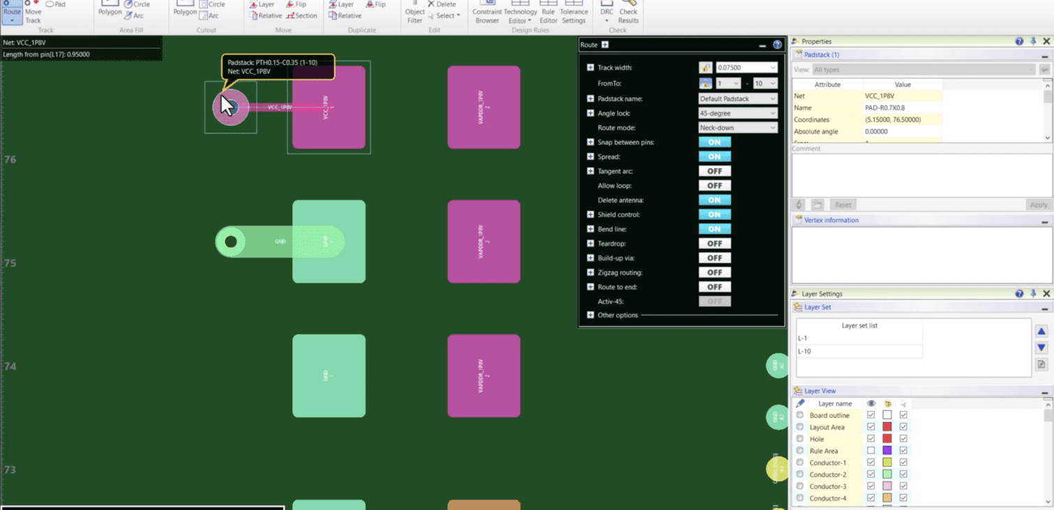
Design Force provides the flexibility to incorporate buried vias into your design rules. The process is straightforward: modify the Via Specification setting from No buried vias to Use predefined buried vias only. This simple change allows for integration into your design workflow.
Specifying Layer Pairs and Qualified Padstack
To further optimize the process, you can automatically assign specific vias for these layers. This involves specifying the layer pairs and the qualified pad stack from layer to layer for each via. By doing so, you ensure that each buried via is correctly placed and functional, adhering to the specific requirements of your design.
Integrating buried vias into your design becomes a seamless process once you have configured your buried vias in Design Force. Setting the Qualified Padstack for the vias expedites and simplifies the routing process between these layers. This step makes the design process more efficient and minimizes the risk of using an incorrect via, ensuring higher accuracy and reliability in your PCB designs.
Video Tutorial: Setting Up Buried Vias in CR-8000 Design Force
We have included a video tutorial below to aid in understanding and implementing this process in your own designs. This video walks you through the entire setup in Design Force, providing visual guidance and practical tips.
Note: This video was recorded using CR-8000 V2023.
In conclusion, using buried vias in your PCB design, particularly when using CR-8000 Design Force, offers a strategic advantage in optimizing complex and compact designs. Following the steps outlined in this blog post and utilizing the video tutorial, you can master the art of buried via implementation, leading to more efficient and innovative PCB designs.


