Introduction: Make Modifying Vias a Breeze
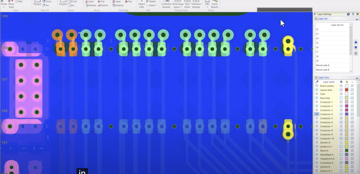
When it comes to PCB design, last-minute changes can be a challenge. However, with CR-8000 Design Force, modifying vias on your already-routed board becomes a breeze. By utilizing the Edit Padstack command conveniently located in the quick access toolbar, Design Force empowers you to quickly and easily make the necessary changes. In this blog post, we’ll walk you through the step-by-step process of swapping vias using Design Force.
Step 1: Add Padstack Editor to the Quick Access Toolbar
First, ensure that the Padstack Editor is added to your quick-access toolbar. This allows for easy access to the necessary tools.
Step 2: Launch the Edit Padstack GUI
Open Design Force and navigate to the quick access toolbar. Click on the Padstack Editor button to launch the Edit Padstack GUI.
Step 3: Select the Via(s) to Change
Identify the specific via(s) that you want to swap out or modify. Use the selection tool to choose the via(s) on your PCB design.
Step 4: Right Mouse Button – “Select all Same Name Padstacks”
To streamline the process, right-click on the selected via(s) and choose the option “Select all Same Name Padstacks.” This ensures that all the vias with the same name are included for modification.
Step 5: Apply Changes Within the Edit Padstack GUI
Locate the Padstack name section, and click the “Apply” button. This will initiate the changes and update the selected vias with the modified padstack properties.
Conclusion
Design Force makes swapping vias a quick and straightforward process, even when you’ve already routed your board. Following these simple steps and utilizing the Edit Padstack command, you can efficiently modify and swap out vias to meet your design requirements. Embrace the convenience and efficiency that Design Force offers, ensuring smooth last-minute changes in your PCB design.
Related Products & Resources
- Blog
- Blog
- Products
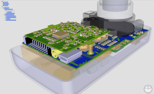
Design Force combines traditional 2D design with native 3D design and the latest human interface techniques, accelerated graphics and almost instantaneous rendering and refreshing. It is the fastest, most effective PCB design solution available today. Design Force enables design teams to layout their designs in the context of a complete system or product.

- Products
Building a competitive product today is much more difficult than a few years ago. Existing PCB-centric design processes are limited to a single PCB and do not provide the necessary tools for today’s competitive product development environment. PCB-centric design processes are falling behind.
