Menu
Improperly configured or disregarded design rules can form sharp angles in wiring routes or at component pads. These angles can lead to unwanted acid traps when fabricating printed circuit boards (PCBs). Acid traps typically occur at junctions where traces meet at sharp angles, causing the etching solution to become trapped. These junctions can occur when a smaller-than-normal gap between the trace and the pad in a high-density or multi-layered PCB or when a small pocket forms during the etching process. It is crucial to adhere to proper design rules to prevent these issues during the fabrication of PCBs.
The steps to configure these ADM checks are as follows:
- Ensure that the DFM Center/ADM for the Design Force module is installed. If you do not have this feature (ZX2301 ADM Basic), you can inquire with your Account Manager about obtaining a trial license if you want to try it out.
- Log in to the Rule Manager, which can be accessed by launching the “Zuken CR-8000 DFM Center 2023 RuleManager” program from the start menu.
- Enable the checks you wish to perform and customize them according to your requirements. The following examples are specific to Acute Wiring.
- Once the checks are defined in the Rule Manager, you can download them to a file with an extension of (xxx.xar). You can choose the name of the file, and it is typically saved in the same location as the xxx.dsgn file.
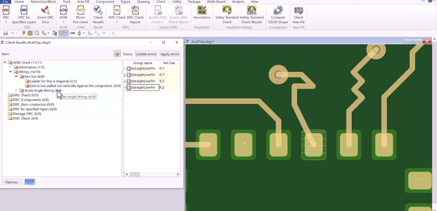
- Open the design you want to run the checks in Design Force. Under the Check Tab, navigate to the ADM icon on the ribbon.
- Click on “ADM Check Settings” and browse to the xxx.xar file that you created in the Rule Manager. Your specific checks will appear in the dialog, and you can select the ones you want to execute.
- You are now ready to execute the ADM checks on your design. Click on the ADM icon to launch the dialog.
- Finally, you can review the Check Results to assess any issues that may have been detected.
The following video demonstrates this process.
This video was recorded in Design Force V2023.


