A good PCB layout is sometimes a work of art. In fact, many of the best PCB designers I know actually have degrees in the arts. Like any good work of art, a certain degree of divine inspiration is necessary to produce an effective and elegant design. With all that said, there are still many physical rules and constraints to follow that the art world doesn’t have to contend with. And then there is a gray area where something may be technically correct, and no physics rules are broken, but it still doesn’t follow the best practices of PCB design. That’s why we went to the experts. We asked them to share their top 5 PCB layout and routing mistakes. Learning from their shared knowledge, we can all advance the art and science of PCB layout.
5) Forgetting What’s Above and Below Your Routes, Ivan, Ubicquia
PCB layout is a 3-dimensional problem. It is easy to become so preoccupied with all the activity happening in a particular layer that you forget there is just as much action above and below. Sometimes the activity several layers away can cause problems in other layers. Consider the example of a high-current, fast-switching power plane. There may be several cutouts on that plane or on the shielding ground planes above and below it. High order harmonics from that power plane could easily couple onto high-speed signals several layers away.
Be on the lookout for long parallel traces running in close proximity above or below sensitive traces. Perpendicular crossing is generally not as problematic as the total area of overlap and coupling is much smaller than a long parallel overlapping run. Even if the overlap is minimal, it is still important to consider the frequency of the respective signals. Keep signals of similar frequencies well apart from each other.
Much is made of PCB dielectric constants, but the story doesn’t end there. The dielectric constant is a good measure of electrical isolation between layers. Other parameters might be just as important. The loss tangent, also called the dissipation factor, is a measure of how much energy is lost due to reactive elements, not unlike the power factor in AC systems. Higher-end PCBs for high-speed signals should have low-loss tangents. But be warned, the loss tangent is frequency-dependent.

4) Putting Test Points in the Wrong Place, Jeff, Ford Motor Company
Test point placement is a highly debatable topic, and there probably isn’t one right answer. That’s the problem–trying to find a one-size-fits-all solution. You can look at this in several ways: From a circuit designer’s point of view of where signals and charges travel down conductors; or from a transmission line designer’s point of view, where electromagnetics and fields reign supreme. Really it all depends on context and frequency where one methodology outweighs another. It helps to think of the charge paradigm with low-speed signals. This is where a signal will experience increasing amounts of degradation as it travels down a conductor. In such cases, it is best to place test points closest to the receiver where you can measure the signal at its most attenuated. If you pass the worst-case condition, then you should be good in all other cases.
Then there is the electromagnetics approach to the problem. This approach is particularly advantageous when thinking about higher frequency signals. Launching a signal down to one end of the conductor is only half of its run. There will be some reflection. Eventually, you come to a standing wave problem, and it might be better to measure near the source where any reflections will interfere with outgoing signals. Often, your worst-case point is actually there near the source. Either way, you’ll determine the placement based on the signals you are measuring. Oh, by the way, beware of long test point stubs as those can cause reflections and negatively impact your signals.

3) Assuming All Grounds Are Created Equal, Marco, Amazon
There is perhaps no magical resolution to your PCB problems other than to throw more ground at it (more on that later). This is where we find another of the most common PCB layout and routing mistakes. It’s not good practice to have one giant ground plane for all your signals (RF, digital, and power) to return through. The reason is that noise on one can–and probably will–couple to all signals. So, we simply create a ground for each type of signal. This approach can be problematic as it may produce large current loops if the only path back is all the way back at the power supply. The various power planes need to be tied together in multiple areas, especially near signals that travel between planes. This step will help keep the inductive loops shorter.

2) Leaving Long Return Loops, Niraj, Magic Leap
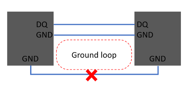
As we stated in mistake #3, it would be nice if all grounds were the same, and it didn’t matter where our signals made it back to their source (yes, I know the idea of current making loops isn’t technically accurate). This isn’t always as easy as ensuring that your signal has the quickest path back to the source. It is easy to miss a possible longer ground return path. There’s no guarantee that long ground loops will cause a problem, but sometimes we can overlook this scenario when other noise mitigation techniques fail. Grounding can work magic to reduce noise, but overgrounding can produce multi-path ground return loops that act as antennas to radiate or capture EMI. To eliminate this issue, place signals and sources close to the source grounds. You can also avoid sharing ground on signals.
And the issue of ground loops isn’t just for PCBs. In test equipment, the chassis are all grounded together, and the bench all shares a common ground. You can pick up signals without really grounding anything, but they’ll be far cleaner if you ground close to where you’re probing.

1. Ignoring Bend Regions, Josh, Lab126
PCB layout and routing mistakes don’t just create challenges with EMI; there are also mechanical challenges. Routing sensitive signals under stress concentrators like shield tracks can cause thin copper traces to break under the stresses of a fall. Flexible circuits enable interesting form factors in today’s electronics, and signals are becoming more and more dense in FPCs. Placing vias in the bend regions of flexes is a recipe for trouble. When dynamic bending takes place, often those small vias break the connection to their signals. Avoid those flex bend vias whenever possible. Similarly, not placing some sort of stiffener under SMT components on a flex will almost surely cause those components to detach from the substrate.

Simulate and Evaluate with eCADSTAR
Best practices and advice are just that. The only real way to know is to build and test, but that’s expensive. Many EDA tools like eCADSTAR provide simulation capabilities to help designers understand potential performance before spending the time and money on building and testing a new PCB. More often than not, most PCB layout and routing mistakes arise when you follow the best practices, but neglect to perform adequate simulation. Try eCADSTAR’s SI/PI engine today and see if you can use some of these tips to improve your designs. Do you have any tough lessons learned you’d like to share with us? Join the conversation on LinkedIn and tell us!
Related Products and Resources

- Blog

- Blog

- Blog

- Blog